SEMICONDUCTOR TECHNICAL DATA
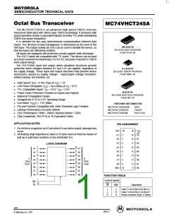
The MC74VHCT245A is an advanced high speed CMOS octal bus
transceiver fabricated with silicon gate CMOS technology. It achieves high
speed operation similar to equivalent Bipolar Schottky TTL while maintaining
CMOS low power dissipation.
It is intended for two–way asynchronous communication between data
buses. The direction of data transmission is determined by the level of the
DIR input. The output enable pin (OE) can be used to disable the device, so
that the buses are effectively isolated.
All inputs are equipped with protection circuits against static discharge.
The VHCT inputs are compatible with TTL levels. This device can be used
as a level converter for interfacing 3.3V to 5.0V, because it has full 5V CMOS
level output swings.
DW SUFFIX
20–LEAD SOIC PACKAGE
CASE 751D–04
The VHCT245A input and output (when disabled) structures provide
protection when voltages between 0V and 5.5V are applied, regardless of
the supply voltage. These input and output structures help prevent device
destruction caused by supply voltage – input/output voltage mismatch,
battery backup, hot insertion, etc.
DT SUFFIX
20–LEAD TSSOP PACKAGE
CASE 948E–02
•
•
•
•
•
•
•
•
•
•
•
High Speed: t
= 4.9ns (Typ) at V
= 5V
PD
Low Power Dissipation: I
CC
= 4µA (Max) at T = 25°C
CC
A
TTL–Compatible Inputs: V = 0.8V; V = 2.0V
Power Down Protection Provided on Inputs and Outputs
Balanced Propagation Delays
Designed for 4.5V to 5.5V Operating Range
IL IH
M SUFFIX
20–LEAD SOIC EIAJ PACKAGE
CASE 967–01
Low Noise: V
= 1.6V (Max)
OLP
ORDERING INFORMATION
Pin and Function Compatible with Other Standard Logic Families
Latchup Performance Exceeds 300mA
ESD Performance: HBM > 2000V; Machine Model > 200V
Chip Complexity: 304 FETs or 76 Equivalent Gates
MC74VHCTXXXADW
MC74VHCTXXXADT
MC74VHCTXXXAM
SOIC
TSSOP
SOIC EIAJ
APPLICATION NOTES
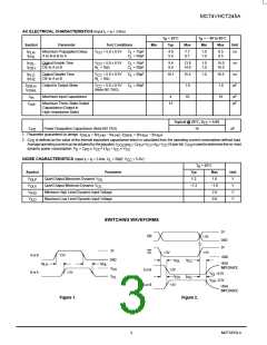
PIN ASSIGNMENT
1. Do not force a signal on an I/O pin when it is an active output, damage may
occur.
DIR
1
20
V
CC
2. All floating (high impedence) input or I/O pins must be fixed by means of
pull up or pull down resistors or bus terminator ICs.
A1
A2
2
3
19
18
OE
B1
A3
4
17
B2
LOGIC DIAGRAM
2
3
4
5
6
7
8
9
18
17
16
15
14
13
12
11
A4
A5
5
16
15
14
13
12
11
B3
B4
B5
B6
B7
B8
A1
A2
A3
A4
A5
A6
A7
A8
B1
B2
B3
B4
B5
B6
B7
B8
6
A6
7
A
DATA
PORT
B
A7
8
DATA
PORT
A8
9
GND
10
FUNCTION TABLE
Control Inputs
1
DIR
OE
19
OE
DIR
Operation
L
L
H
L
H
X
Data Tx from Bus B to Bus A
Data Tx from Bus A to Bus B
Buses Isolated (High–Z State)
6/97
Motorola, Inc. 1997
REV 0
1

 ONSEMI [ ONSEMI ]