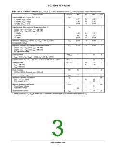
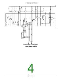
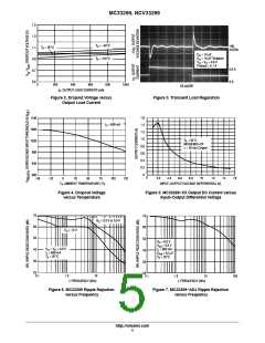
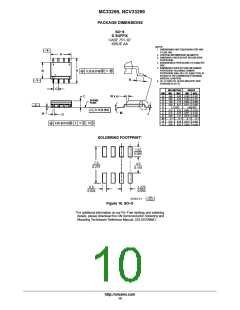
MC33269, NCV33269
APPLICATIONS INFORMATION
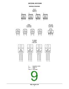
Figures 11 through 15 are typical application circuits. The
supply input filter with long wire lengths. This will reduce
the circuit’s sensitivity to the input line impedance at high
frequencies. A 0.33 mF or larger tantalum, mylar, ceramic,
or other capacitor having low internal impedance at high
frequencies should be chosen. The bypass capacitor should
be mounted with shortest possible lead or track length
directly across the regulator’s input terminals. Applications
should be tested over all operating conditions to insure
stability.
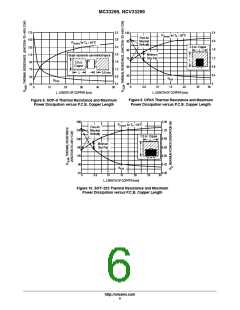
Internal thermal limiting circuitry is provided to protect
the integrated circuit in the event that the maximum junction
temperature is exceeded. When activated, typically at
170°C, the output is disabled. There is no hysteresis built
into the thermal limiting circuit. As a result, if the device is
overheating, the output will appear to be oscillating. This
feature is provided to prevent catastrophic failures from
accidental device overheating. It is not intended to be used
as a substitute for proper heat−sinking.
output current capability of the regulator is in excess of
800 mA, with a typical dropout voltage of less than 1.0 V.
Internal protective features include current and thermal
limiting.
* The MC33269 requires an external output capacitor for
stability. The capacitor should be at least 10 mF with an
equivalent series resistance (ESR) of less than 10 W but
greater than 0.2 W over the anticipated operating
temperature range. With economical electrolytic capacitors,
cold temperature operation can pose a problem. As
temperature decreases, the capacitance also decreases and
the ESR increases, which could cause the circuit to oscillate.
Also capacitance and ESR of a solid tantalum capacitor is
more stable over temperature. The use of a low ESR ceramic
capacitor placed within close proximity to the output of the
device could cause instability.
** An input bypass capacitor is recommended to improve
transient response or if the regulator is connected to the
V
in
V
out
V
in
V
out
MC33269
MC33269−XX
**
C
in
*
10 mF
C
**
o
C
in
R1
R2
*
C
Adj
o
10 mF
GND
An input capacitor is not necessary for stability, however
it will improve the overall performance.
C
Adj
***
Figure 11. Typical Fixed Output Application
R2
ꢀ + ꢀ1.25ꢀꢀǒ1 ) Ǔꢀ)ꢀ I
V
R2
Adjꢀ
out
R1
***C is optional, however it will improve the ripple rejection.
Adj
V
R
S
I
out
in
The MC34269 develops a 1.25 V reference voltage between the
output and the adjust terminal. Resistor R1, operates with
constant current to flow through it and resistor R2. This current
should be set such that the Adjust Pin current causes negligible
drop across resistor R2. The total current with minimum load
should be greater than 8.0 mA.
MC33269
*
10 mF
C
o
**
C
in
Adj
1.25
R
I
ꢀ +ꢀ
out
S
Figure 13. Current Regulator
Figure 12. Typical Adjustable Output Application
V
in
V
out
MC33269−XX
**
C
in
V
in
V
out
MC33269
GND
**
C
in
R1
R2
Adj
*
C
o
10 mF
MC33269−XX
*
C
o
10 mF
**
C
in
GND
The Schottky diode in series with the ground leg of the upper
regulator shifts its output voltage higher by the forward
voltage drop of the diode. This will cause the lower device
to remain off until the input voltage is removed.
R
sets the maximum output voltage. Each transistor
2
reduces the output voltage when turned on.
Figure 14. Battery Backed−Up Power Supply
Figure 15. Digitally Controlled Voltage Regulator
http://onsemi.com
7

 ONSEMI [ ONSEMI ]