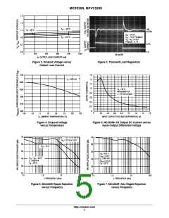
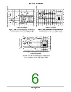
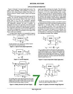
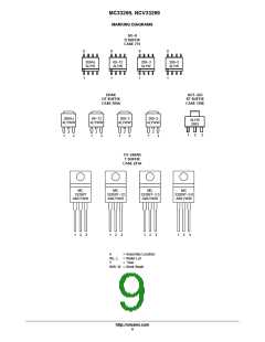
MC33269, NCV33269
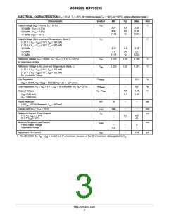
ELECTRICAL CHARACTERISTICS (C = 10 mF, T = 25°C, for min/max values T = −40°C to +125°C, unless otherwise noted.)
O
A
A
Characteristic
Symbol
Min
Typ
Max
Unit
Output Voltage (I = 10 mA, T = 25°C)
V
O
V
out
A
3.27
4.95
3.3
5.0
12
3.33
5.05
3.3 Suffix (V = 5.3 V)
CC
5.0 Suffix (V = 7.0 V)
CC
11.88
12.12
12 Suffix (V = 14 V)
CC
Output Voltage (Line, Load and Temperature) (Note 1)
(1.25 V ≤ V − V ≤ 15 V, I = 500 mA)
V
O
V
in
out
out
(1.35 V ≤ V − V ≤ 10 V, I = 800 mA)
in
out
out
3.3 Suffix
5.0 Suffix
12 Suffix
3.23
4.9
3.3
5.0
12
3.37
5.1
11.76
12.24
Reference Voltage (I = 10 mA, V − V = 2.0 V, T = 25°C)
V
V
1.235
1.25
1.265
V
V
out
in
out
A
ref
for Adjustable Voltage
Reference Voltage (Line, Load and Temperature) (Note 1)
(1.25 V ≤ V − V ≤ 15 V, I = 500 mA)
1.225
1.25
1.275
ref
in
out
out
(1.35 V ≤ V − V ≤ 10 V, I = 800 mA)
in
out
out
for Adjustable Voltage
Line Regulation
Reg
−
−
−
−
0.3
0.5
%
line
(I = 10 mA, V = [V + 1.5 V] to V = 20 V, T = 25°C)
out
in
out
in
A
Load Regulation (V = V + 3.0 V, I = 10 mA to 800 mA, T = 25°C)
Reg
%
V
in
out
out
A
load
Dropout Voltage
(I = 500 mA)
V
in
− V
1.0
1.1
1.25
1.35
out
−
−
out
(I = 800 mA)
out
Ripple Rejection
RR
55
−
−
−
−
dB
(10 V , 120 Hz Sinewave; I = 500 mA)
pp
out
Current Limit (V − V = 10 V)
I
800
mA
mA
in
out
Limit
Quiescent Current (Fixed Output)
(1.5 V ≤ V ≤ 3.3 V)
I
Q
−
−
5.5
−
8.0
20
out
(5 V ≤ V ≤ 12 V)
out
Minimum Required Load Current
Fixed Output Voltage
I
mA
Load
−
−
−
0
−
Adjustable Voltage
8.0
Adjustment Pin Current
I
−
−
120
mA
Adj
1. The MC33269−12, V − V is limited to 8.0 V maximum, because of the 20 V maximum rating applied to V
in.
in
out
http://onsemi.com
3

 ONSEMI [ ONSEMI ]