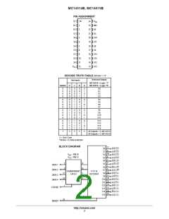
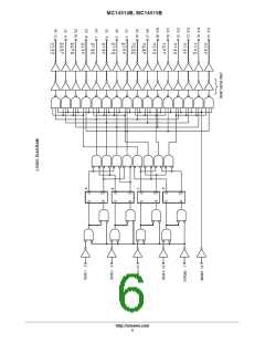
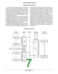
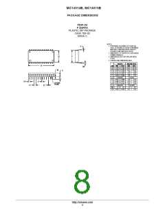
MC14514B, MC14515B
SWITCHING CHARACTERISTICS (6.) (C = 50 pF, T = 25 C)
L
A
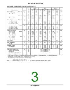
All Types
(7.)
Characteristic
Symbol
V
DD
Unit
Min
Typ
Max
Output Rise Time
t
ns
TLH
THL
t
t
t
= (3.0 ns/pF) C + 30 ns
= (1.5 ns/pF) C + 15 ns
= (1.1 ns/pF) C + 10 ns
5.0
10
15
—
—
—
180
90
65
360
180
130
TLH
TLH
TLH
L
L
L
Output Fall Time
t
ns
ns
ns
ns
t
t
t
= (1.5 ns/pF) C + 25 ns
= (0.75 ns/pF) C + 12.5 ns
= (0.55 ns/pF) C + 9.5 ns
5.0
10
15
—
—
—
100
50
40
200
100
80
THL
THL
THL
L
L
L
Propagation Delay Time; Data, Strobe to S
t ,
PLH
t
t
t
, t
= (1.7 ns/pF) C + 465 ns
= (0.86 ns/pF) C + 192 ns
L
= (0.5 ns/pF) C + 125 ns
L
t
5.0
10
15
—
—
—
550
225
150
1100
450
300
PLH PHL
L
PHL
, t
PLH PHL
, t
PLH PHL
Inhibit Propagation Delay Times
t
,
PLH
t
t
t
, t
= (1.7 ns/pF) C + 315 ns
= (0.66 ns/pF) C + 117 ns
L
= (0.5 ns/pF) C + 75 ns
L
t
PHL
5.0
10
15
—
—
—
400
150
100
800
300
200
PLH PHL
L
, t
PLH PHL
, t
PLH PHL
Setup Time
Data to Strobe
t
su
5.0
10
15
250
100
75
125
50
38
—
—
—
Hold Time
Strobe to Data
t
5.0
10
15
– 20
0
10
– 100
– 40
– 30
—
—
—
ns
ns
h
Strobe Pulse Width
t
WH
5.0
10
15
350
100
75
175
50
38
—
—
—
6. The formulas given are for the typical characteristics only at 25 C.
7. Data labelled “Typ” is not to be used for design purposes but is intended as an indication of the IC’s potential performance.
V
DD
V
DS
S0
S1
STROBE
INHIBIT
D1
For MC14515B
1. For P–channel: Inhibit = V
2. For N–channel: Inhibit = V
2. and D1–D4 constitute binary
2. code for “output under test.”
S2
DD
S3
S4
SS
For MC14514B
S5
S6
1. For P–channel: Inhibit = V
1. and D1–D4 constitute
1. binary code for “output
1. under test.”
SS
S7
S8
D2
S9
I
D
S10
S11
S12
S13
S14
S15
2. For N–channel: Inhibit = V
DD
D3
EXTERNAL
POWER SUPPLY
D4
V
SS
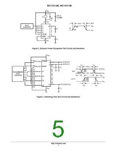
Figure 1. Drain Characteristics Test Circuit
http://onsemi.com
4

 ONSEMI [ ONSEMI ]