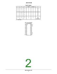
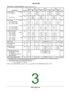
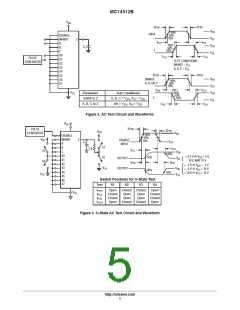
MC14512B
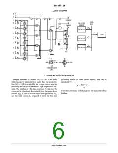
LOGIC DIAGRAM
13
12
C
B
15
11
1
DISABLE
10
A
DATA
BUS
X0
SELECTED
DEVICE
INHIBIT
2
3
4
5
6
7
9
V
I
DD
OD
X1
X2
MC14512B
MC14512B
MC14512B
I
L
LOAD
14
Z
I
TL
X3
X4
X5
X6
I
TL
V
SS
X7
1
1
OUT
IN
IN
OUT
2
2
TRANSMISSION
GATE
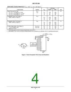
3–STATE MODE OF OPERATION
Output terminals of several MC14512B 8–Bit Data
Selectors can be connected to a single date bus as shown.
One MC14512B is selected by the 3–state control, and the
remaining devices are disabled into a high–impedance “off”
state. The number of 8–bit data selectors, N, that may be
connected to a bus line is determined from the output drive
(including fanout to other device inputs), and can be
calculated by:
IOD – IL
N =
+ 1
ITL
N must be calculated for both high and low logic state of the
bus line.
current, I , 3–state or disable output leakage current, I
,
TL
OD
and the load current, I , required to drive the bus line
L
http://onsemi.com
6

 ONSEMI [ ONSEMI ]