MC14512B
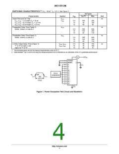
SWITCHING CHARACTERISTICS (7.) (C = 50 pF, T = 25 C, See Figure 1)
L
A
All Types
(8.)
Characteristic
Output Rise and Fall Time
Symbol
V
DD
Typ
Max
Unit
t
,
ns
TLH
t
t
t
, t
= (1.5 ns/pF) C + 25 ns
t
5.0
10
15
100
50
40
200
100
80
TLH THL
L
THL
, t
= (0.75 ns/pF) C + 12.5 ns
TLH THL
L
, t
= (0.55 ns/pF) C + 9.5 ns
L
TLH THL
Propagation Delay Time (Figure 2)
Inhibit, Control, or Data to Z
t
ns
ns
ns
PLH
5.0
10
15
330
125
85
650
250
170
Propagation Delay Time (Figure 2)
Inhibit, Control, or Data to Z
t
PHL
5.0
10
15
330
125
85
650
250
170
3–State Output Delay Times (Figure 3)
“1” or “0” to High Z, and
t
t
, t
, t
,
5.0
10
15
60
35
30
150
100
75
PHZ PLZ
PZH PZL
High Z to “1” or “0”
7. The formulas given are for the typical characteristics only at 25 C.
8. Data labelled “Typ” is not to be used for design purposes but is intended as an indication of the IC’s potential performance.
I
D
V
DD
DISABLE
INHIBIT
A
B
Z
C
L
C
X0
X1
X2
X3
X4
X5
X6
X7
PULSE
GENERATOR
V
in
50%
50%
DUTY
CYCLE
V
SS
Figure 1. Power Dissipation Test Circuit and Waveform
http://onsemi.com
4

 ONSEMI [ ONSEMI ]