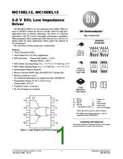
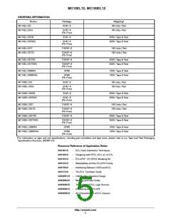
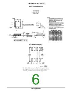
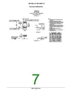
MC10EL12, MC100EL12
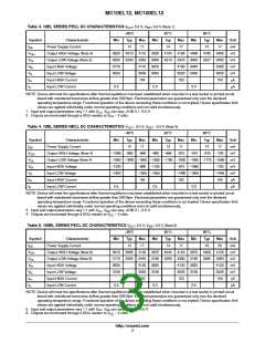
Table 6. 100EL SERIES NECL DC CHARACTERISTICS V = 0.0 V; V = −5.0 V (Note 7)
CC
EE
−40°C
Typ
14
25°C
Typ
14
85°C
Typ
16
Symbol
Characteristic
Power Supply Current
Min
Max
Min
Max
Min
Max
20
Unit
mA
mV
I
EE
17
17
V
V
V
V
Output HIGH Voltage (Note 8)
Output LOW Voltage (Note 8)
Input HIGH Voltage
−1085 −1005 −880 −1025 −955
−880 −1025 −955
−880
OH
OL
IH
−1830 −1695 −1555 −1810 −1705 −1620 −1810 −1705 −1620 mV
−1165
−1810
−880 −1165
−1475 −1810
150
−880 −1165
−1475 −1810
150
−880
mV
Input LOW Voltage
−1475 mV
IL
I
Input HIGH Current
150
mA
mA
IH
IL
I
Input LOW Current
0.5
0.5
0.5
NOTE: Device will meet the specifications after thermal equilibrium has been established when mounted in a test socket or printed circuit
board with maintained transverse airflow greater than 500 lfpm. Electrical parameters are guaranteed only over the declared
operating temperature range. Functional operation of the device exceeding these conditions is not implied. Device specification limit
values are applied individually under normal operating conditions and not valid simultaneously.
7. Input and output parameters vary 1:1 with V . V can vary +0.8 V / −0.5 V.
CC
EE
8. Outputs are terminated through a 50 W resistor to V − 2 volts.
CC
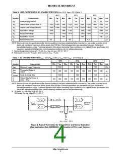
Table 7. AC CHARACTERISTICS V = 5.0 V; V = 0.0 V or V = 0.0 V; V = −5.0 V (Note 9)
CC
EE
CC
EE
−40°C
25°C
Typ
85°C
Typ
Min
Typ
Max
Min
Max
Min
Max
Symbol
Characteristic
Unit
f
Maximum Toggle Frequency
TBD
TBD
TBD
GHz
max
t
t
Propagation Delay to
Output
PLH
PHL
120
280
TBD
350
500
180
290
TBD
350
450
210
320
TBD
350
480
ps
ps
ps
t
Cycle−to−Cycle Jitter
JITTER
t
r
t
f
Output Rise/Fall Times Q
(20% − 80%)
150
550
150
550
150
550
NOTE: Device will meet the specifications after thermal equilibrium has been established when mounted in a test socket or printed circuit
board with maintained transverse airflow greater than 500 lfpm. Electrical parameters are guaranteed only over the declared
operating temperature range. Functional operation of the device exceeding these conditions is not implied. Device specification limit
values are applied individually under normal operating conditions and not valid simultaneously.
9. 10 Series: V can vary +0.06 V / −0.5 V.
EE
100 Series: V can vary +0.8 V / −0.5 V.
EE
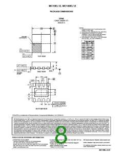
Z = 50 W
Q
D
D
o
Receiver
Device
Driver
Device
Q
Z = 50 W
o
50 W
50 W
V
TT
V
TT
= V − 3.0 V
CC
Figure 2. Typical Termination for Output Driver and Device Evaluation
(See Application Note AND8020/D − Termination of ECL Logic Devices.)
http://onsemi.com
4

 ONSEMI [ ONSEMI ]