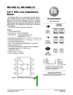
MC10EL12, MC100EL12
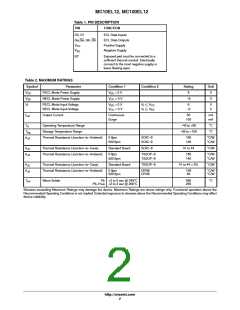
Table 1. PIN DESCRIPTION
PIN
FUNCTION
D0, D1
ECL Data Inputs
ECL Data Outputs
Positive Supply
Negative Supply
Qa,Qa; Qb, Qb
V
CC
V
EE
EP
Exposed pad must be connected to a
sufficient thermal conduit. Electrically
connect to the most negative supply or
leave floating open.
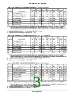
Table 2. MAXIMUM RATINGS
Symbol
Parameter
PECL Mode Power Supply
NECL Mode Power Supply
Condition 1
Condition 2
Rating
Unit
V
V
V
EE
V
CC
= 0 V
= 0 V
8
CC
EE
I
V
V
−8
V
PECL Mode Input Voltage
NECL Mode Input Voltage
V
V
= 0 V
= 0 V
V ꢀ V
6
−6
V
V
EE
I
CC
V ꢁ V
CC
I
EE
I
Output Current
Continuous
Surge
50
100
mA
mA
out
T
Operating Temperature Range
−40 to +85
°C
°C
A
T
Storage Temperature Range
−65 to +150
stg
JA
q
Thermal Resistance (Junction−to−Ambient)
0 lfpm
500 lfpm
SOIC−8
SOIC−8
190
130
°C/W
°C/W
q
q
Thermal Resistance (Junction−to−Case)
Thermal Resistance (Junction−to−Ambient)
Standard Board
SOIC−8
41 to 44
°C/W
JC
JA
0 lfpm
500 lfpm
TSSOP−8
TSSOP−8
185
140
°C/W
°C/W
q
q
Thermal Resistance (Junction−to−Case)
Thermal Resistance (Junction−to−Ambient)
Standard Board
TSSOP−8
41 to 44 ± 5%
°C/W
JC
JA
0 lfpm
500 lfpm
DFN8
DFN8
129
84
°C/W
°C/W
T
sol
Wave Solder
Pb <2 to 3 sec @ 248°C
Pb−Free <2 to 3 sec @ 260°C
265
265
°C
Stresses exceeding Maximum Ratings may damage the device. Maximum Ratings are stress ratings only. Functional operation above the
Recommended Operating Conditions is not implied. Extended exposure to stresses above the Recommended Operating Conditions may affect
device reliability.
http://onsemi.com
2

 ONSEMI [ ONSEMI ]