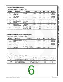
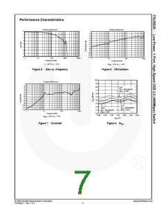
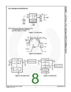
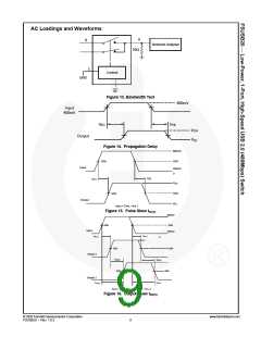
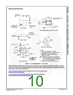
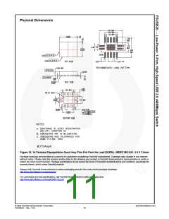
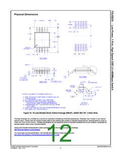
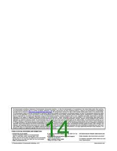
Physical Dimensions
0.10
C
2.10
A
2X
1.62
B
KEEPOUT ZONE, NO TRACES
OR VIAS ALLOWED
(0.11)
0.56
1.12
1.60
PIN1 IDENT IS
2X LONGER THAN
OTHER LINES
0.10
C
10X
(0.35)
(0.25)
2X
10X
0.50
TOP VIEW
RECOMMENDED LAND PATTERN
0.55 MAX
0.05 C
0.05 C
0.05
0.00
(0.20)
C
0.35
0.25
SIDE VIEW
(0.15)
D
DETAIL A
(0.36)
0.35
0.25
0.65
0.55
0.35
0.25
DETAIL A 2X SCALE
1
4
0.56
NOTES:
10
5
A. PACKAGE CONFORMS TO JEDEC
REGISTRATION MO-255, VARIATION UABD .
B. DIMENSIONS ARE IN MILLIMETERS.
C. DIMENSIONS AND TOLERANCES PER
ASME Y14.5M, 1994.
D. PRESENCE OF CENTER PAD IS PACKAGE
SUPPLIER DEPENDENT. IF PRESENT IT
IS NOT INTENDED TO BE SOLDERED AND
HAS A BLACK OXIDE FINISH.
(0.29)
0.35
6
9
9X
0.25
0.50
0.25
0.15
9X
1.62
0.10
0.05
C
C
A B
ALL FEATURES
E. DRAWING FILENAME: MKT-MAC10Arev5.
BOTTOM VIEW
Figure 17. 10-Lead MicroPak™, 1.6 x 2.1mm
Package drawings are provided as a service to customers considering Fairchild components. Drawings may change in any manner
without notice. Please note the revision and/or date on the drawing and contact a Fairchild Semiconductor representative to verify or
obtain the most recent revision. Package specifications do not expand the terms of Fairchild’s worldwide terms and conditions, specifically the
warranty therein, which covers Fairchild products.
Always visit Fairchild Semiconductor’s online packaging area for the most recent package drawings:
http://www.fairchildsemi.com/packaging/
For current tape and reel specifications, visit Fairchild Semiconductor’s online packaging area:
http://www.fairchildsemi.com/products/logic/pdf/micropak_tr.pdf.
© 2005 Fairchild Semiconductor Corporation
FSUSB20 • Rev. 1.0.3
www.fairchildsemi.com
9

 ONSEMI [ ONSEMI ]