Layout Considerations
General layout and supply bypassing play a major role
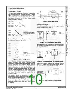
The selection of the coupling capacitor is a function of the
subsequent circuit input impedance and the leakage
current of the input being driven. To obtain the highest
quality output video signal, the series termination resistor
must be placed as close to the device output pin as
possible. This greatly reduces the parasitic capacitance
and inductance effect on the output driver. The distance
from the device pin to the series termination resistor
should be no greater than 2.54mm (0.1in).
in
high-frequency
performance
and
thermal
characteristics. Fairchild offers a four-layer board with
full power and ground planes board to guide layout and
aid device evaluation. The demo board is a four-layer
board with full power and ground planes. Following this
layout configuration provides optimum performance and
thermal characteristics for the device. For best results,
follow the steps and recommended routing rules below.
Recommended Routing / Layout Rules
.
.
Do not run analog and digital signals in parallel.
Use separate analog and digital power planes to
supply power.
.
Traces should run on top of the ground plane at all
times.
.
.
.
No trace should run over ground/power splits.
Avoid routing at 90-degree angles.
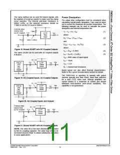
Figure 22. Termination Resistor Placement
Minimize clock and video data trace length
differences.
.
.
.
.
.
Include 10μF and 0.1μF ceramic power supply
bypass capacitors.
Thermal Considerations
Since the interior of most systems, such as set-top
boxes, TVs, and DVD players; are at +70ºC;
consideration must be given to providing an adequate
heat sink for the device package for maximum heat
dissipation. When designing a system board, determine
how much power each device dissipates. Ensure that
devices of high power are not placed in the same
location, such as directly above (top plane) or below
(bottom plane) each other, on the PCB.
Place the 0.1μF capacitor within 2.54mm (0.1in)
of the device power pin.
Place the 10μF capacitor within 19.05mm (0.75in)
of the device power pin.
For multi-layer boards, use a large ground plane to
help dissipate heat.
For two-layer boards, use a ground plane that
extends beyond the device body at least 12.7mm
(0.5in) on all sides. Include a metal paddle under
the device on the top layer.
PCB Thermal Layout Considerations
.
Minimize all trace lengths to reduce series
inductance.
.
Understand the system power requirements and
environmental conditions.
.
.
Maximize thermal performance of the PCB.
Output Considerations
The outputs are DC offset from the input by 150mV
therefore VOUT = 2 • VIN DC + 150mV. This offset is
required for optimal performance from the output driver
and is held at the minimum value to decrease the
standing DC current into the load. Since the FMS6144A
has a 2x (6dB) gain, the output is typically connected via
a 75ꢀ series back-matching resistor followed by the
75ꢀ video cable. Because of the inherent divide by two
of this configuration, the blanking level at the load of the
video signal is always less than 1V. When AC-coupling
the output, ensure that the coupling capacitor passes
the lowest frequency content in the video signal and that
line time distortion (video tilt) is kept as low as possible.
Consider using 70μm of copper for high-power
designs.
.
.
.
.
Make the PCB as thin as possible by reducing FR4
thickness.
Use vias in power pad to tie adjacent layers
together.
Remember that baseline temperature is a function
of board area, not copper thickness.
Modeling techniques provide a first-order
approximation.
© 2009 Fairchild Semiconductor Corporation
FMS6144A • Rev. 1.0.2
www.fairchildsemi.com
11

 ONSEMI [ ONSEMI ]