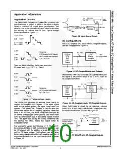
The same method can be used for biased signals, with
the addition of a pull-up resistor to make sure the clamp
never operates. The internal pull-down resistance is
800kꢀ ±20%, so the external resistance should be
7.5Mꢀ to set the DC level to 500mV.
Power Dissipation
The output drive configuration must be considered when
calculating overall power dissipation. Care must be taken
not to exceed the maximum die junction temperature. The
following example can be used to calculate the power
dissipation and internal temperature rise.
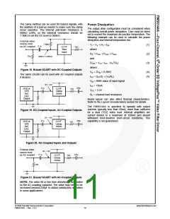
External video
source must
be AC coupled
7.5Mꢀ
TJ = TA + PD • JA
where:
(1)
(2)
(3)
0.1μ
LCVF
Bias
Input
75ꢀ
PD = PCH1 + PCH2 + PCH3
and
PCHX = VCC • ICH - (VO2/RL)
75ꢀ
500mV +/-350mV
where:
Figure 18. Biased SCART with DC-Coupled Outputs
VO = 2VIN + 0.280V
ICH = (ICC/3) + (VO/RL)
VIN = RMS value of input signal
ICC = 19mA
(4)
(5)
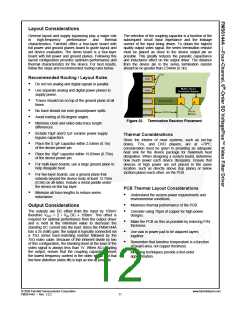
The same circuits can be used with AC-coupled outputs
if desired.
0V - 1.4V
0.1μ
220μ
DVD or
STB
SoC
LCVF
Clamp
Active
75ꢀ
VCC = 3.3V.
RL = channel load resistance
DAC
Output
Board layout can also affect thermal characteristics.
Refer to the Layout Considerations section for details.
The FMS6144A is specified to operate with output
currents typically less than 50mA, more than sufficient
for a dual (75ꢀ) video load. Internal amplifiers are
current limited to a maximum of 100mA and should
withstand brief-duration short-circuit conditions. This
capability is not guaranteed.
Figure 19. DC-Coupled Inputs, AC-Coupled Outputs
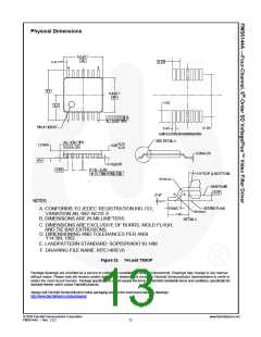
0V - 1.4V
0.1μ
220μ
DVD or
STB
SoC
LCVF
Clamp
Active
75ꢀ
DAC
Output
Figure 20. AC-Coupled Inputs and Outputs
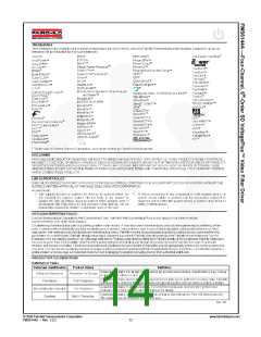
External video
0V - 1.4V
source must
be AC coupled
0.1μ
220μ
LCVF
Clamp
Active
75ꢀ
75ꢀ
Figure 21. Biased SCART with AC-Coupled Outputs
NOTE: The video tilt or line time distortion is dominated
by the AC-coupling capacitor. The value may need to be
increased beyond 220μF to obtain satisfactory operation
in some applications.
© 2009 Fairchild Semiconductor Corporation
FMS6144A • Rev. 1.0.2
www.fairchildsemi.com
10

 ONSEMI [ ONSEMI ]