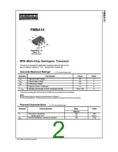
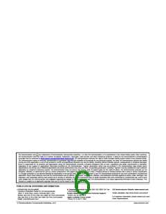
FMBA14
C2
E1
C1
B2
E2
B1
pin #1
SuperSOT -6
Mark: .1N
Dot denotes pin #1
NPN Multi-Chip Darlington Transistor
This device is designed for applications requiring extremely high current
gain at collector currents to 1.0 A. Sourced from Process 05.
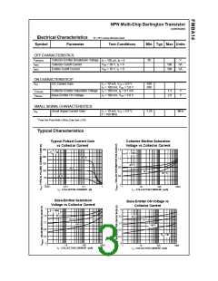
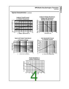
Absolute Maximum Ratings*
TA = 25°C unless otherwise noted
Symbol
Parameter
Value
Units
VCES
VCBO
VEBO
IC
Collector-Emitter Voltage
Collector-Base Voltage
Emitter-Base Voltage
30
V
V
V
A
30
10
4
Collector Current - Continuous
1.2
Operating and Storage Junction Temperature Range
-55 to +150
C
°
TJ, Tstg
*These ratings are limiting values above which the serviceability of any semiconductor device may be impaired.
NOTES:
1) These ratings are based on a maximum junction temperature of 150 degrees C.
2) These are steady state limits. The factory should be consulted on applications involving pulsed or low duty cycle operations.
Thermal Characteristics
TA = 25°C unless otherwise noted
Symbol
Characteristic
Max
Units
FMBA14
PD
Total Device Dissipation
Derate above 25°C
Thermal Resistance, Junction to Ambient
700
5.6
180
mW
mW/°C
°C/W
RθJA
1998 Fairchild Semiconductor Corporation

 ONSEMI [ ONSEMI ]