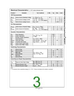
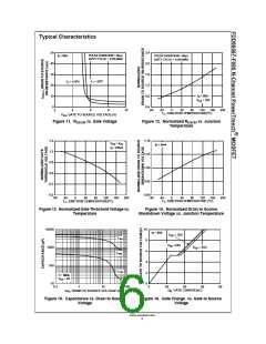
Electrical Characteristics TJ = 25°C unless otherwise noted.
Symbol
Parameter
Test Conditions
Min.
Typ.
Max.
Units
Off Characteristics
BVDSS
IDSS
Drain-to-Source Breakdown Voltage
Drain-to-Source Leakage Current
Gate-to-Source Leakage Current
ID = 250μA, VGS = 0V
60
-
-
-
-
-
-
1
V
V
DS= 6 0 V , T J = 25oC
μA
mA
nA
VGS = 0V
TJ = 175oC (Note 4)
-
1
IGSS
VGS = ±20V
-
±100
On Characteristics
VGS(th)
RDS(on)
Gate to Source Threshold Voltage
Drain to Source On Resistance
VGS = VDS, ID = 250μA
2
-
2.9
2.6
4.9
4
V
TJ = 25oC
3.2
6.0
mΩ
mΩ
ID = 80A,
TJ = 175oC (Note 4)
-
V
GS= 10V
Dynamic Characteristics
Ciss
Input Capacitance
-
-
-
-
-
-
-
-
4950
1300
45
-
-
pF
pF
pF
Ω
V
DS = 30V, VGS = 0V,
Coss
Crss
Rg
Output Capacitance
f = 1MHz
Reverse Transfer Capacitance
Gate Resistance
-
VGS = 0.5V, f = 1MHz
VGS = 0 to 10V
2.3
63
-
Qg(ToT)
Qg(th)
Qgs
Total Gate Charge
82
-
nC
nC
nC
nC
VDD = 48V
ID = 80A
Threshold Gate Charge
Gate-to-Source Gate Charge
Gate-to-Drain “Miller“ Charge
VGS = 0 to 2V
9.1
24
-
Qgd
10
-
Switching Characteristics
ton
td(on)
tr
Turn-On Time
Turn-On Delay
Rise Time
-
-
-
-
-
-
-
105
ns
ns
ns
ns
ns
ns
24
45
32
13
-
-
-
V
DD = 30V, ID = 80A,
VGS = 10V, RGEN = 6Ω
td(off)
tf
Turn-Off Delay
Fall Time
-
-
toff
Turn-Off Time
59
Drain-Source Diode Characteristics
I
SD = 80A, VGS = 0V
ISD = 40A, VGS = 0V
DD = 48V, IF = 80A,
dISD/dt = 100A/μs
-
-
-
-
-
1.25
1.2
89
V
VSD
Source-to-Drain Diode Voltage
-
V
trr
Reverse-Recovery Time
68
76
ns
nC
V
Qrr
Reverse-Recovery Charge
114
Note:
4: The maximum value is specified by design at T = 175°C. Product is not tested to this condition in production.
J
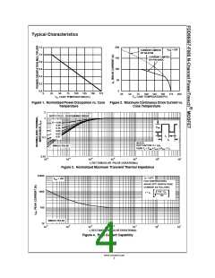
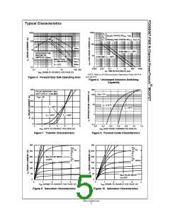
www.onsemi.com
2

 ONSEMI [ ONSEMI ]