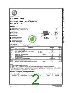
FDD86567-F085
®
N-Channel PowerTrench MOSFET
60 V, 100 A, 3.2 mΩ
Features
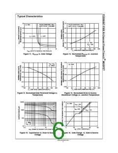
Typical R
= 2.6 mΩ at V = 10V, I = 80 A
GS D
DS(on)
D
Typical Q
= 63 nC at V = 10V, I = 80 A
g(tot)
GS
D
UIS Capability
RoHS Compliant
Qualified to AEC Q101
D
G
G
Applications
S
D-PAK
TO-252
(TO-252)
Automotive Engine Control
PowerTrain Management
Solenoid and Motor Drivers
Integrated Starter/Alternator
Primary Switch for 12V Systems
S
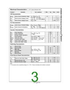
MOSFET Maximum Ratings TJ = 25°C unless otherwise noted.
Symbol
VDSS
Parameter
Ratings
60
Units
Drain-to-Source Voltage
Gate-to-Source Voltage
V
V
VGS
±20
Drain Current - Continuous (VGS=10) (Note 1)
Pulsed Drain Current
TC = 25°C
TC = 25°C
100
ID
A
See Figure 4
115
EAS
PD
Single Pulse Avalanche Energy
(Note 2)
mJ
W
W/oC
oC
oC/W
oC/W
Power Dissipation
Derate Above 25oC
227
1.52
TJ, TSTG Operating and Storage Temperature
-55 to + 175
0.66
RθJC
RθJA
Thermal Resistance, Junction to Case
Maximum Thermal Resistance, Junction to Ambient
(Note 3)
52
Notes:
1: Current is limited by bondwire configuration.
2: Starting T = 25°C, L = 40μH, I = 76A, V = 60V during inductor charging and V = 0V during time in avalanche.
J
AS
DD
DD
3: R
is the sum of the junction-to-case and case-to-ambient thermal resistance, where the case thermal reference is defined as the solder
θJA
mounting surface of the drain pins.
presented here is based on mounting on a 1 in pad of 2oz copper.
R
is guaranteed by design, while R is determined by the board design. The maximum rating
θJC θJA
2
Package Marking and Ordering Information
Device Marking
Device
Package
Reel Size
Tape Width
Quantity
FDD86567
FDD86567-F085
D-PAK(TO-252)
13”
16mm
2500units
©2015 Semiconductor Components Industries, LLC.
August-2017,Rev. 2
Publication Order Number:
FDD86567-F085/D

 ONSEMI [ ONSEMI ]