FDC6401N
TYPICAL CHARACTERISTICS (continued)
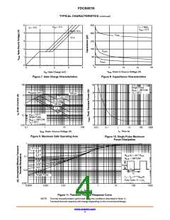
5
4
450
V
DS
= 5 V
f = 1 MHz
= 0 V
I
D
= 3 A
V
GS
10 V
360
C
ISS
15 V
3
2
1
0
270
180
C
OSS
90
0
C
RSS
0
5
10
, Drain to Source Voltage (V)
20
0
2
15
1
3
4
V
Q , Gate Charge (nC)
DS
g
Figure 7. Gate Charge Characteristics
Figure 8. Capacitance Characteristics
100
10
8
Single Pulse
R
= 180°C/W
q
JA
R
Limit
T = 25°C
A
DS(ON)
100 ms
10
1
1 ms
10 ms
6
100 ms
1 s
4
2
0
DC
V
= 4.5 V
GS
0.1
0.01
Single Pulse
= 180°C/W
R
q
JA
T = 25°C
A
1
10
100
0.01
0.1
1
10
100
1000
0.1
t , Time (s)
1
V
DS
, Drain−Source Voltage (V)
Figure 9. Maximum Safe Operating Area
Figure 10. Single Pulse Maximum
Power Dissipation
1
D = 0.5
0.2
0.1
R
R
(t) = r(t) * R
= 180°C/W
q
q
q
JA
JA
JA
0.1
0.05
0.02
0.01
P(pk)
t
1
0.01
t
2
Single Pulse
T − T = P * R (t)
q
JA
J
A
Duty Cycle, D = t /t
1
2
0.001
0.0001
0.001
0.01
0.1
t , Time (s)
1
10
100
1000
1
Figure 11. Transient Thermal Response Curve
NOTE: Thermal characterization performed using the conditions described in Note 1c.
Transient thermal response will change depending on the circuit board design.
www.onsemi.com
4

 ONSEMI [ ONSEMI ]