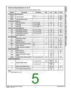
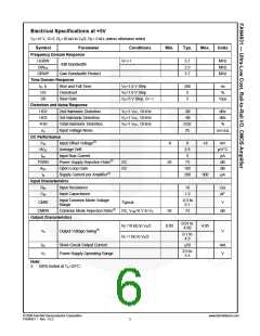
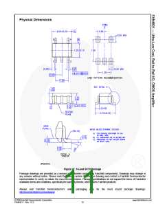
Application Information
General Description
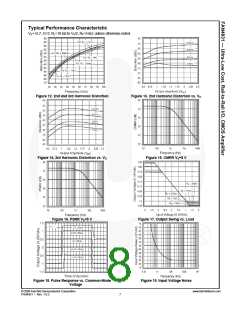
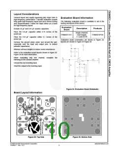
Overdrive Recovery
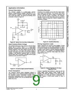
The FAN4931 amplifier is a single-supply, general-
purpose, voltage-feedback amplifier, fabricated on a bi-
CMOS process. It features a rail-to-rail input and output
and is unity gain stable. The typical non-inverting circuit
schematic is shown in Figure 20.
Overdrive of an amplifier occurs when the output and/or
input ranges are exceeded. The recovery time varies
based on whether the input or output is overdriven and
by how much the range is exceeded. The FAN4931
typically recovers in less than 500 ns from an overdrive
condition. Figure 22 shows the FAN4931 amplifier in an
overdriven condition.
Figure 22. Overdrive Recovery
Figure 20. Typical Non-Inverting Configuration
Driving Capacitive Loads
Input Common-Mode Voltage
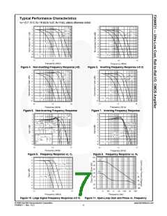
Figure 8 illustrates the response of the amplifier. A small
series resistance (RS) at the output, illustrated in Figure
23, improves stability and settling performance. RS values
in Figure 8 were chosen to achieve maximum bandwidth
with less than 2 dB of peaking. For maximum flatness,
use a larger RS. Capacitive loads larger than 500 pF
require the use of RS.
The common-mode input range extends to 300 mV below
ground and to 100 mV above VS in single-supply
operation. Exceeding these values does not cause phase
reversal; however, if the input voltage exceeds the rails
by more than 0.5 V, the input ESD devices begin to
conduct. The output stays at the rail during this overdrive
condition. If the absolute maximum input VIN (700 mV
beyond either rail) is exceeded, externally limit the input
current to ±5 mA, as shown in Figure 21.
Figure 23. Typical Topology for Driving a
Capacitive Load
Figure 21. Circuit for Input Current Protection
Power Dissipation
Driving a capacitive load introduces phase-lag into the
output signal, which reduces phase margin in the
amplifier. The unity gain follower is the most sensitive
configuration. In a unity gain follower configuration, the
amplifier requires a 300 Ω−series resistor to drive a
100 pF load.
The maximum internal power dissipation allowed is
directly related to the maximum junction temperature. If
the maximum junction temperature exceeds 150°C,
performance degradation occurs. If the maximum junction
temperature exceeds 150°C for an extended time, device
failure may occur.
© 2008 Fairchild Semiconductor Corporation
FAN4931 • Rev. 1.0.2
www.fairchildsemi.com
8

 ONSEMI [ ONSEMI ]