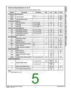
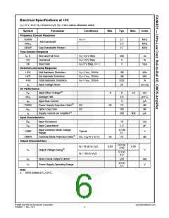
Layout Considerations
General layout and supply bypassing play major roles in
high-frequency performance. Fairchild evaluation boards
help guide high-frequency layout and aid in device testing
and characterization. Follow the steps below as a basis
for high-frequency layout:
Evaluation Board Information
The following evaluation board is available to aid in the
testing and layout of this device.
Evaluation
Description
Products
Include 6.8 μF and 0.01 μF ceramic capacitors.
Board
Place the 6.8 μF capacitor within 0.75 inches of the
power pin.
Single-Channel,
Dual-Supply,
FAN4931-011
FAN4931IP5X
5 -Lead SC70
Place the 0.01 μF capacitor within 0.1 inches of the
power pin.
Evaluation board schematics are shown in Figure 24;
layouts are shown in Figure 25-Figure 26.
Remove the ground plane under and around the part,
especially near the input and output pins, to reduce
parasitic capacitance.
Minimize all trace lengths to reduce series inductances.
Refer to the evaluation board layouts shown in Figure 24-
Figure 26 for more information.
When evaluating only one channel, complete the
following on the unused channel:
Ground the non-inverting input.
Short the output to the inverting input.
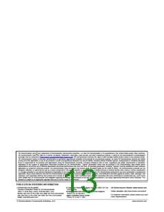
Figure 24. Evaluation Board Schematic
Board Layout Information
Figure 25. Top Side
Figure 26. Bottom Side
© 2008 Fairchild Semiconductor Corporation
FAN4931 • Rev. 1.0.2
www.fairchildsemi.com
9

 ONSEMI [ ONSEMI ]