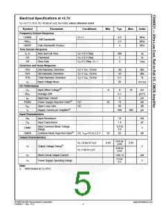
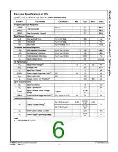
Electrical Specifications at +2.7V
VS=+2.7 V, G=2, RL=10 kΩ to VS/2, RF=5 kΩ; unless otherwise noted.
Symbol
Parameter
Conditions
Min.
Typ.
Max.
Units
Frequency Domain Response
UGBW
G=+1
4.0
2.5
4
MHz
MHz
MHz
-3dB Bandwidth
BWSS
GBWP
Gain Bandwidth Product
Time Domain Response
tR, fF
OS
Rise and Fall Time
VO=1.0 V Step
300
5
ns
%
Overshoot
Slew Rate
VO=1.0 V Step
SR
VO=3 V Step, G=-1
3
V/µs
Distortion and Noise Response
HD2
2nd Harmonic Distortion
VO=1 VPP, 10 kHz
VO=1 VPP, 10 kHz
VO=1 VPP, 10 kHz
-66
-67
0.1
26
dBc
dBc
HD3
3rd Harmonic Distortion
Total Harmonic Distortion
Input Voltage Noise
THD
%
en
nV/√Hz
DC Performance
VIO
dVIO
Ibn
Input Offset Voltage(2)
-6
0
2.1
5
+6
mV
µV/°C
pA
Average Drift
Input Bias Current
PSRR
AOL
IS
Power Supply Rejection Ratio(2)
DC
DC
50
73
98
200
dB
Open-Loop Gain
Supply Current per Amplifier(2)
dB
300
µA
Input Characteristics
RIN
CIN
Input Resistance
10
GΩ
Input Capacitance
1.4
pF
Input Common Mode Voltage
Range
-0.3 to
2.8
CMIR
V
CMRR
Common Mode Rejection Ratio(2)
DC, VCM=OV to 2.2 V
50
65
dB
Output Characteristics
0.01 to
2.69
0.03
2.65
RL=10 kΩ to VS/2
RL=1 kΩ to VS/2
VO
Output Voltage Swing(2)
V
0.05 to
2.55
ISC
VS
Short-Circuit Output Current
+34/-12
mA
V
2.5 to
5.5
Power Supply Operating Range
Note:
2. 100% tested at TA=25°C.
© 2008 Fairchild Semiconductor Corporation
FAN4931 • Rev. 1.0.2
www.fairchildsemi.com
4

 ONSEMI [ ONSEMI ]