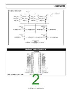
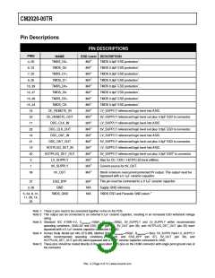
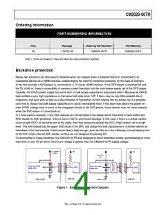
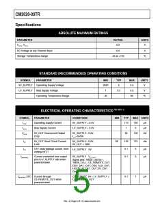
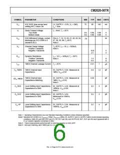
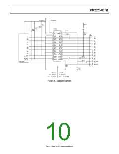
CM2020-00TR
SYMBOL
PARAMETER
CONDITIONS
MIN
TYP
MAX UNITS
VON
VOLTAGE drop across level
shifting NFET when ON
LV_SUPPLY = 2.5V, VS = GND,
IDS = 3mA
75
95
140
mV
VF
Diode Forward Voltage
Top Diode
Bottom Diode
IF = 8mA, TA = 25°C
0.6
0.6
0.85
0.85
0.95
0.95
V
V
VESD
ESD Withstand Voltage, contact
discharge per IEC 61000-4-2
standard (IEC)
Pins 4, 7, 10, 13, 20, 21, 22, 23, 24,
27, 30, 33, 38; TA=25°C
Note 2
kV
8
VCL
Channel Clamp Voltage
Positive Transients
Negative Transients
TA=25°C, IPP = 1A, tP = 8/20uS;
Note 3
10.8
-2.1
V
V
RDYN
Dynamic Resistance
Positive Transients
Negative Transients
IPP = 1A, tP = 8/20µS; TA = 25°C;
1.4
0.9
Ω
Ω
Note 3
ILEAK
TMDS Channel Leakage Current TA = 25°C
0.01
1
µA
CIN, TMDS
TMDS Channel Input
Capacitance
5V_SUPPLY= 5.0V, Measured at
1MHz, VBIAS=2.5V
0.9
1.2
pF
TMDS Channel Input
Capacitance Matching
5V_SUPPLY= 5.0V, Measured at
1MHz, VBIAS=2.5V;
Note 4
0.05
3.5
pF
pF
pF
∆
CIN, TMDS
CIN, DDC
Level Shifting Input Capacitance, 5V_SUPPLY= 5.0V, Measured at
100KHz, VBIAS=2.5V;
Note 2
4
4
Capacitance to GND
CIN, CEC
Level Shifting Input Capacitance, 5V_SUPPLY= 5.0V,
Measured at 100KHz,
VBIAS=2.5V
3.5
Capacitance to GND
CIN, HP
Level Shifting Input Capacitance, 5V_SUPPLY= 5.0V, Measured at
Capacitance to GND 100KHz, VBIAS=2.5V
3.5
4
pF
Note 1: Operating Characteristics are over Standard Operating Conditions unless otherwise specified.
Note2: Standard IEC 61000-4-2, CDISCHARGE=150pF, RDISCHARGE=330 , 5V_SUPPLY and LV_SUPPLY within recommended operating
Ω
conditions, GND=0V and ESD_BYP (pin 37), 5V_OUT (pin 38), and HOTPLUG_DET_OUT (pin 20) each bypassed with a
0.1µF ceramic capacitor connected to GND.
Note 3: These measurements performed with no external capacitor on ESD_BYP.
Note 4: Intra-pair matching, each TMDS pair (i.e. D+, D-)
Rev. 4 | Page 6 of 13 | www.onsemi.com

 ONSEMI [ ONSEMI ]