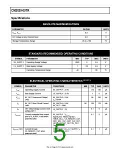
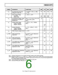
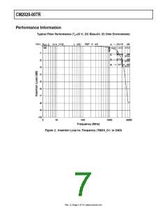
CM2020-00TR
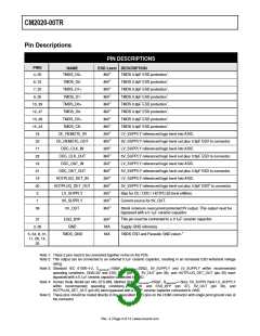
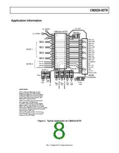
Pin Descriptions
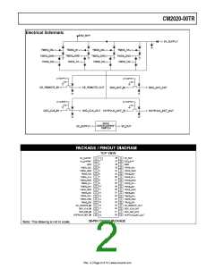
PIN DESCRIPTIONS
PINS
4, 35
6, 33
7, 32
9, 30
10, 29
12, 27
13, 26
15, 24
16
NAME
ESD Level DESCRIPTION
TMDS_D2+
8kV3
8kV3
8kV3
8kV3
8kV3
8kV3
8kV3
8kV3
2kV4
8kV3
2kV4
8kV3
2kV4
8kV3
2kV4
8kV3
2kV4
2kV4
8kV3
TMDS 0.9pF ESD protection1.
TMDS_D2-
TMDS_D1+
TMDS 0.9pF ESD protection1.
TMDS 0.9pF ESD protection1.
TMDS_D1-
TMDS 0.9pF ESD protection1.
TMDS_D0+
TMDS 0.9pF ESD protection1.
TMDS_D0-
TMDS 0.9pF ESD protection1.
TMDS_CK+
TMDS 0.9pF ESD protection1.
TMDS_CK-
TMDS 0.9pF ESD protection1.
CE_REMOTE_IN
CE_REMOTE_OUT
DDC_CLK_IN
DDC_CLK_OUT
DDC_DAT_IN
DDC_DAT_OUT
HOTPLUG_DET_IN
HOTPLUG_DET_OUT
LV_SUPPLY
LV_SUPPLY referenced logic level into ASIC.
5V_SUPPLY referenced logic level out plus 3.5pF ESD to connector.
LV_SUPPLY referenced logic level into ASIC.
5V_SUPPLY referenced logic level out plus 3.5pF ESD to connector.
LV_SUPPLY referenced logic level into ASIC.
5V_SUPPLY referenced logic level out plus 3.5pF ESD to connector.
LV_SUPPLY referenced logic level into ASIC.
5V_SUPPLY referenced logic level out plus 3.5pF ESD2 to connector
Bias for CE / DDC / HOTPLUG level shifters.
Current source for 5V_OUT.
23
17
22
18
21
19
20
2
1
5V_SUPPLY
38
5V_OUT
55mA minimum overcurrent protected 5V output. This output must be
bypassed with a 0.1µF ceramic capacitor.
2kV4
N/A
N/A
This pin must be connected to a 0.1µF ceramic capacitor.
37
ESD_BYP
GND
3, 36
Supply GND reference.
5, 34, 8, 31,
11, 28, 14,
25
TMDS_GND
TMDS ESD and Parasitic GND return.5
Note 1: These 2 pins need to be connected together in-line on the PCB.
Note 2: This output can be connected to an external 0.1µF ceramic capacitor, resulting in an increased ESD withstand voltage
rating.
Note 3: Standard IEC 61000-4-2, CDISCHARGE=150pF, RDISCHARGE=330Ω, 5V_SUPPLY and LV_SUPPLY within recommended
operating conditions, GND=0V and ESD_BYP (pin 37), 5V_OUT (pin 38), and HOTPLUG_DET_OUT (pin 20) each
bypassed with a 0.1µF ceramic capacitor connected to GND.
Note 4: Human Body Model per MIL-STD-883, Method 3015, CDISCHARGE=100pF, RDISCHARGE=1.5kΩ, 5V_SUPPLYand LV_SUPPLY
within recommended operating conditions, GND=0V and ESD_BYP (pin 37), 5V_OUT (pin 38), and
HOTPLUG_DET_OUT (pin 20) each bypassed with a 0.1µF ceramic capacitor connected to GND.
Note 5: These pins should be routed directly to the associated GND pins on the HDMI connector with single point ground vias at
the connector
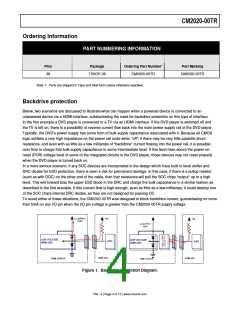
Rev. 4 | Page 3 of 13 | www.onsemi.com

 ONSEMI [ ONSEMI ]