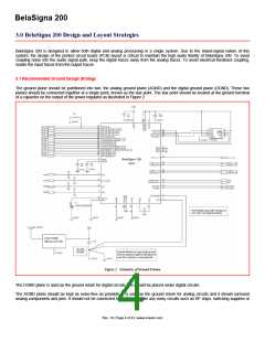
BelaSigna 200
4.1.2. QFN Pad Out
Pad # Pad Name
Pad Function
Charge pump capacitor pin 0
Double voltage
Audio signal input to ADC0
Audio signal input to ADC0/line level output signal from preamp 0
Reference voltage for microphone
Audio signal input to ADC1
Audio signal input to ADC1
Regulated voltage for microphone bias
Analog ground
I/O
N/A
O
U/D
N/A
N/A
N/A
N/A
N/A
N/A
N/A
N/A
N/A
N/A
N/A
N/A
N/A
1
CAP0
2
VDBL
3
A|0
I
4
5
A|1/LOUT
A|R
I/O
N/A
I
I
O
N/A
I
N/A
O
6
A|2
7
A|3
8
9
10
11
12
13
VREG
AGND
AI_RC
AOR
AO1/RCVR1-
AO0/RCVR1+
Remote control input
Reference voltage for DAC
Audio signal output from DAC1/output from direct digital drive 1-
Audio signal output from DAC0/output from direct digital drive 1+
O
Pad # Pad Name
Pad Function
Positive power supply
Output from direct digital drive 0
Output from direct digital drive 0
Receiver return current
General-purpose I/O/clock divider reset/I2S interface
analog blocks frame output
General-purpose I/O/I2S interface analog blocks input
General-purpose I/O/I2S interface analog blocks input
General-purpose I/O/I2S interface digital blocks frame
Digital pads supply input
I/O
I
O
O
N/A
U/D
N/A
N/A
N/A
N/A
14
15
16
17
VBAT
RCVR0-
RCVR0+
RCVRGND
GPIO[3]/
18
I/O
U
NCLK_DIV_RESET/I2S_FA
GPIO[2]/I2S_INA
GPIO[1]/I2S_IND
GPIO[0]/I2S_FD
VDDO
GNDO
EXT_CLK
DEBUG_RX
DEBUG_TX
19
20
21
22
23
24
25
26
I/O
I/O
I/O
I
N/A
I/O
I
U
U
U
N/A
N/A
U
Digital pads ground
External clock input/internal clock output
Debug port receive
U
U
Debut port transmit
O
Pad # Pad Name
Pad Function
I/O
N/A
I/O
I
N/A
O
U/D
N/A
U
27
28
29
30
31
32
33
34
35
36
37
38
39
RESERVED
TWSS_SDA
TWSS_CLK
GNDC
VDDC
SPI_SERO
SPI_SERI
SPI_CS
SPI_CLK
GPIO[15]
TWSS data
TWSS clock
Core logic ground
U
N/A
N/A
D
U
D
N/A
U
U
U
U
Core logic, EEPROM and pad supply output
Serial peripheral interface serial data out
Serial peripheral interface serial data in
Serial peripheral interface chip select
Serial peripheral interface clock
General-purpose I/O
General-purpose I/O/PCM interface frame
General-purpose I/O/PCM interface output
General-purpose I/O/PCM interface input
I/O
I
I/O
I/O
I/O
I/O
I/O
I/O
GPIO[14]/PCM_FRAME
GPIO[13]/PCM_OUT
GPIO[12]/PCM_IN
Pad # Pad Name
Pad Function
No connection
No connection
General-purpose I/O/PCM interface clock
Digital pads ground
I/O
N/A
N/A
I/O
N/A
I
U/D
N/A
N/A
U
N/A
N/A
U
40
41
42
43
44
45
N/C
N/C
GPIO[11]/PCM_CLK
GNDO
VDDO
Digital pads supply input
GPIO[10]/DCLK
General-purpose I/O/class D receiver clock
Low-speed A/D/general-purpose I/O/general-purpose
UART receive
Low-speed A/D input/general-purpose I/O/general-
purpose UART transmit
I/O
46
47
LSAD[5]/GPIO[9]/UART_RX
LSAD[4]/GPIO[8]/UART_TX
I/O
I/O
U
U
48
49
LSAD[3]/GPIO[7]
LSAD[2]/GPIO[6]
Low-speed A/D input/general purpose I/P
Low-speed A/D input/general purpose I/P
Low-speed A/D inputs/general-purpose I/O/I2S interface
analog blocks output
I/O
I/O
U
U
50
LSAD[1]/GPIO[5]/I2S_OUTA
I/O
U
Low-speed A/D inputs/general-purpose I/O/I2S interface
analog blocks output
Charge pump capacitor pin 1
51
52
LSAD[0]/GPIO[4]/I2S_OUTD
CAP1
I/O
U
N/A
N/A
Rev. 16 | Page 8 of 43 | www.onsemi.com

 ONSEMI [ ONSEMI ]