BelaSigna 200
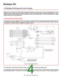
digital pads of BelaSigna 200 itself. Analog ground returns associated with the audio output stage should connect back to the star point
on separate individual traces.
For more information on the recommended ground design strategy, see Table 1.
In some designs, space constraints may make separate ground planes impractical. In this case a star configuration strategy should be
used. Each analog ground return should connect to the star point with separate traces.
3.2 Internal Power Supplies
Power management circuitry in BelaSigna 200 generates separate digital (VDDC) and analog (VREG, VDBL) regulated supplies. Each
supply requires an external decoupling capacitor, even if the supply is not used externally. Decoupling capacitors should be placed as
close as possible to the power pads. Further details are provided in Table 1. Non-critical signals are outlined in Table 2.
Table 1: Critical Signal
Pin Name
Description
Routing Guideline
Place 1μF (min) decoupling capacitor close to pin. Connect negative
terminal of capacitor to DGND plane.
VBAT
Power supply
Place separate 1μF decoupling capacitors close to each pin. Connect
negative capacitor terminal to AGND. Keep away from digital traces and
output traces. VREG may be used to generate microphone bias. VDBL
shall not be used to supply external circuitry.
Internal regulator for analog
sections
VREG, VDBL
AGND
VDDC
Analog ground return
Connect to AGND plane.
Place 10μF decoupling capacitor close to pin. Connect negative terminal
of capacitor to DGND. Should be connected to VDDO pins and to
EEPROM power.
Internal regulator for digital
sections
Digital ground return (pads and
core)
GNDO, GNDC
Connect to digital ground.
Keep as short as possible. Keep away from all digital traces and audio
outputs. Avoid routing in parallel with other traces. Connect unused inputs
to AGND.
Microphone inputs
AI0, AI1 / LOUT, AI2, AI3
Connect to AGND. If no analog ground plane, should share trace with
microphone grounds to star point.
AIR
Input stage reference voltage
Analog audio output
AO0, AO1
Keep away from microphone inputs.
RCVR0+, RCVR0-, RCVR1+,
RCVR1-
Keep away from analog traces, particularly microphone inputs.
Corresponding traces should be of approximately the same length.
Direct digital audio output
AOR
Output stage reference voltage
Output stage ground return
Connect to star point. Share trace with power amplifier (if present).
Connect to star point.
RCVRGND
External clock input / internal
clock output
Minimize trace length. Keep away from analog signals. If possible,
surround with digital ground.
EXT_CLK
AI_RC
Infrared receiver input
If used, minimize trace length to photodiode.
Rev. 16 | Page 5 of 43 | www.onsemi.com

 ONSEMI [ ONSEMI ]