CP1E-E@@D@-@ CP1E-N@@D@-@/NA20D@-@
●Output Specifications for Transistor Outputs (Sinking or Sourcing)
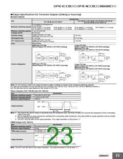
Normal Outputs
Specification
CIO 100.02 to CIO 100.07, CIO 101.00 to CIO 101.07
and CIO 102.00 to CIO 102.07 *2
Item
CIO 100.00 and CIO 100.01
0.3 A/output, 0.9 A/common *1
4.5 to 30 VDC
CP1E-E10D@-@: 0.9 A/Unit
CP1E-N40D@-@: 3.6 A/Unit
Maximum switching capacity
CP1E-N14D@-@: 1.5 A/Unit
CP1E-N60D@-@: 5.4 A/Unit
CP1E-N20D@-@: 1.8 A/Unit
CP1E-NA20D@-@: 1.8 A/Unit
CP1E-N30D@-@: 2.7 A/Unit
Minimum switching capacity 1 mA 4.5 to 30 VDC
Leakage current
Residual voltage
ON response time
OFF response time
Fuse
0.1mA max.
E-type CPU Unit: 1.5 V max.
N/NA-type CPU Unit: 0.6 V max.
1.5V max.
0.1 ms max.
1 ms max.
0.1 ms max.
E-type CPU Unit: 1 ms max.
N/NA-type CPU Unit: 0.1 ms max.
Not provided.
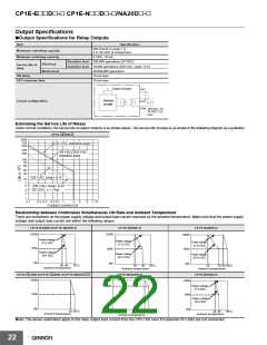
N/NA-type CPU Unit:
E-type CPU Unit:
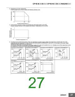
Normal outputs CIO 100.00 to CIO 100.01 (sinking)
Normal outputs CIO 100.00 to CIO 100.03 (sinking)
N/NA-type CPU Unit:
Normal outputs CIO 100.02 to CIO 102.07 (sinking)
OUT
L
OUT
L
OUT
L
OUT
L
Internal
circuits
24 VDC,
4.5 to 30
VDC
24 VDC,
4.5 to 30
VDC
Internal
circuits
Internal
circuits
COM(–)
COM(–)
N/NA-type CPU Unit:
Normal outputs CIO 100.00 to CIO 100.01 (sourcing)
Circuit configuration
E-type CPU Unit:
Normal outputs CIO 100.01 to CIO 100.03 (sourcing)
N/NA-type CPU Unit:
Normal outputs CIO 100.02 to CIO 102.07 (sourcing)
COM(+)
COM(+)
24 VDC,
4.5 to 30
VDC
Internal
circuits
Internal
circuits
Internal
circuits
24 VDC,
4.5 to 30
VDC
OUT
OUT
L
L
OUT
OUT
L
L
Note: Do not connect a load to an output terminal or apply a voltage in excess of the maximum switching capacity.
* 1 Also do not exceed 0.9 A for the total for CIO 100.00 to CIO 100.03. (CIO 100.00 to CIO 100.03 is different common.)
* 2 The bits that can be used depend on the model of CPU Unit.
Pulse Outputs (CIO 100.00 and CIO 100.01)
Item
Specification
Maximum switching capacity
Minimum switching capacity
Maximum output frequency
100 mA/4.5 to 26.4 VDC
7 mA/4.5 to 26.4 VDC
100 kHz
OFF 90
%
Output waveform
ON 10
%
4µs min.
2µs min.
Note: 1. The load for the above values is assumed to be the resistance load, and does not take into account the impedance for the connecting
cable to the load.
2. Due to distortions in pulse waveforms resulting from connecting cable impedance, the pulse widths in actual operation may be smaller
than the values shown above.
3. The OFF and ON refer to the output transistor. The output transistor is ON at level “L”.
PWM Output (CIO 100.01)
Item
Specification
Maximum switching capacity
Maximum output frequency
30 mA/4.5 to 26.4 VDC
32 kHz
For ON duty +1%, .0%:10 kHz output
For ON duty +5%, .0%: 0 to 32 kHz output
PWM output accuracy
Output waveform
OFF
ON
t
ON
t
ON
ON duty=
×
100%
T
T
Note: The OFF and ON refer to the output transistor. The output transistor is ON at level “L”.
23

 OMRON [ OMRON ELECTRONICS LLC ]