TDA8920C
NXP Semiconductors
2 × 110 W class-D power amplifier
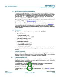
8.2 Pulse-width modulation frequency
The amplifier output signal is a PWM signal with a typical carrier frequency of between
250 kHz and 450 kHz. A 2nd-order LC demodulation filter on the output is used to convert
the PWM signal into an analog audio signal. The carrier frequency is determined by an
external resistor, ROSC, connected between pins OSC and VSSA. The optimal carrier
frequency setting is between 250 kHz and 450 kHz.
The carrier frequency is set to 345 kHz by connecting an external 30 kΩ resistor between
pins OSC and VSSA. See Table 9 on page 14 for more details.
If two or more class-D amplifiers are used in the same audio application, it is
recommended that an external clock circuit be used with all devices (see Section 13.4).
This will ensure that they operate at the same switching frequency, thus avoiding beat
tones (if the switching frequencies are different, audible interference known as ‘beat tones’
can be generated)
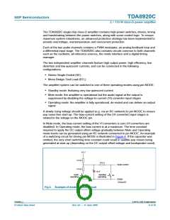
8.3 Protection
The following protection circuits are incorporated into the TDA8920C:
• Thermal protection:
– Thermal FoldBack (TFB)
– OverTemperature Protection (OTP)
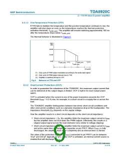
• OverCurrent Protection (OCP)
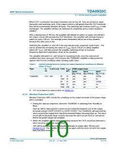
• Window Protection (WP)
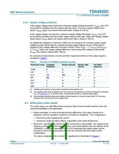
• Supply voltage protection:
– UnderVoltage Protection (UVP)
– OverVoltage Protection (OVP)
– UnBalance Protection (UBP)
How the device reacts to a fault conditions depends on which protection circuit has been
activated.
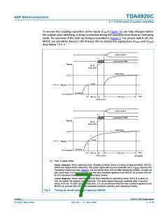
8.3.1 Thermal protection
The TDA8920C employes an advanced thermal protection strategy. A TFB function
gradually reduces the output power within a defined temperature range. If the temperature
continues to rise, OTP is activated to shut down the device completely.
8.3.1.1 Thermal FoldBack (TFB)
If the junction temperature (Tj) exceeds the thermal foldback activation threshold, the gain
is gradually reduced. This reduces the output signal amplitude and the power dissipation,
eventually stabilizing the temperature.
TFB is specified at the thermal foldback activation temperature Tact(th_fold) where the
closed-loop voltage gain is reduced by 6 dB. The TFB range is:
T
act(th_fold) − 5 °C < Tact(th_fold) < Tact(th_prot)
The value of Tact(th_fold) for the TDA8920C is approximately 153 °C; see Table 8 for more
details.
TDA8920C_2
© NXP B.V. 2009. All rights reserved.
Product data sheet
Rev. 02 — 11 June 2009
8 of 39

 NXP [ NXP ]