TDA8920C
NXP Semiconductors
2 × 110 W class-D power amplifier
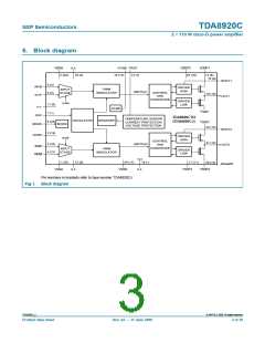
The TDA8920C single-chip class-D amplifier contains high-power switches, drivers, timing
and handshaking between the power switches, along with some control logic. To ensure
maximum system robustness, an advanced protection strategy has been implemented to
provide overvoltage, overtemperature and overcurrent protection.
Each of the two audio channels contains a PWM modulator, an analog feedback loop and
a differential input stage. The TDA8920C also contains circuits common to both channels
such as the oscillator, all reference sources, the mode interface and a digital timing
manager.
The two independent amplifier channels feature high output power, high efficiency, low
distortion and low quiescent currents, and can be connected in the following
configurations:
• Stereo Single-Ended (SE)
• Mono Bridge-Tied Load (BTL)
The amplifier system can be switched to one of three operating modes using pin MODE:
• Standby mode: featuring very low quiescent current
• Mute mode: the amplifier is operational but the audio signal at the output is
suppressed by disabling the voltage-to-current (VI) converter input stages
• Operating mode: the amplifier is fully operational, de-muted and can deliver an output
signal
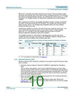
A slowly rising voltage should be applied (e.g. via an RC network) to pin MODE to ensure
pop noise-free start-up. The bias-current setting of the (VI converter) input stages is
related to the voltage on the MODE pin.
In Mute mode, the bias-current setting of the VI converters is zero (VI converters are
disabled). In Operating mode, the bias current is at a maximum. The time constant
required to apply the DC output offset voltage gradually between Mute and Operating
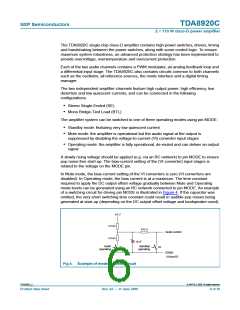
mode levels can be generated using an RC network connected to pin MODE. An example
of a switching circuit for driving pin MODE is illustrated in Figure 4. If the capacitor was
omitted, the very short switching time constant could result in audible pop noises being
generated at start-up (depending on the DC output offset voltage and loudspeaker used).
+
5 V
5.6 kΩ
470 Ω
mode control
5.6 kΩ
10 µF
mute/
operating
standby/
operating
S1
S2
SGND
010aaa552
Fig 4. Example of mode selection circuit
TDA8920C_2
© NXP B.V. 2009. All rights reserved.
Product data sheet
Rev. 02 — 11 June 2009
6 of 39

 NXP [ NXP ]