TDA8920C
NXP Semiconductors
2 × 110 W class-D power amplifier
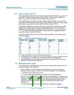
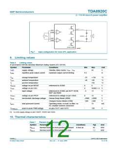
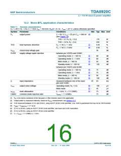
OUT1
IN1P
IN1M
V
SGND
OUT2
in
IN2P
IN2M
power stage
mbl466
Fig 7.
Input configuration for mono BTL application
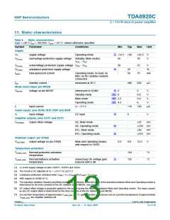
9. Limiting values
Table 6.
Limiting values
In accordance with the Absolute Maximum Rating System (IEC 60134).
Symbol
Parameter
Conditions
Min
-
Max
65
-
Unit
V
[1]
VP
supply voltage
Standby, Mute modes; VDD − VSS
maximum output current limiting
IORM
repetitive peak output current
9.2
A
Tstg
Tamb
Tj
storage temperature
ambient temperature
junction temperature
voltage on pin MODE
voltage on pin OSC
input voltage
−55
−40
-
+150
+85
°C
°C
°C
V
150
VMODE
VOSC
VI
referenced to SGND
0
6
0
SGND + 6
+5
V
referenced to SGND; pin IN1P; IN1M;
IN2P and IN2M
−5
V
VPROT
VESD
voltage on pin PROT
referenced to voltage on pin VSSD
Human Body Model (HBM)
0
12
V
electrostatic discharge voltage
−2000 +2000
V
Charged Device Model (CDM)
−500
+500
75
V
Iq(tot)
total quiescent current
Operating mode; no load; no filter; no
RC-snubber network connected
-
mA
VPWM(p-p)
peak-to-peak PWM voltage
on pins OUT1 and OUT2
-
120
V
[1] VP is the supply voltage on pins VDDP1, VDDP2 and VDDA.
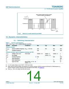
10. Thermal characteristics
Table 7.
Symbol
Rth(j-a)
Thermal characteristics
Parameter
Conditions
Typ
40
Unit
K/W
K/W
thermal resistance from junction to ambient in free air
thermal resistance from junction to case
Rth(j-c)
1.1
TDA8920C_2
© NXP B.V. 2009. All rights reserved.
Product data sheet
Rev. 02 — 11 June 2009
12 of 39

 NXP [ NXP ]