TDA8920C
NXP Semiconductors
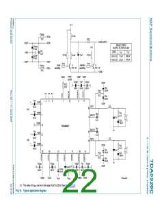
2 × 110 W class-D power amplifier
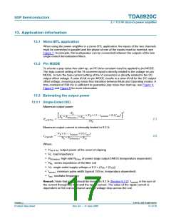
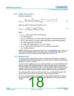
13.3.2 Bridge-Tied Load (BTL)
Maximum output power:
2
R
L
× 2V × (1 – t
× 0.5 f
)
osc
-------------------------------------------------------------------
P
w(min)
R + R + R
L
DSon(hs)
DSon(ls)
P
=
(3)
(4)
-----------------------------------------------------------------------------------------------------------------------------------------------------------
2R
o(0.5%)
L
Maximum output current internally limited to 9.2 A:
2V × (1 – t
× 0.5 f
)
osc
P
w(min)
I
=
------------------------------------------------------------------------------------------
R + (R + R ) + 2R
o(peak)
L
DSon(hs)
DSon(ls)
sL
Where:
• Po(0.5 %): output power at the onset of clipping
• RL: load impedance
• RDSon(hs): high-side RDSon of power stage output DMOS (temperature dependent)
• RDSon(ls): low-side RDSson of power stage output DMOS (temperature dependent)
• RsL: series impedance of the filter coil
• VP: single-sided supply voltage or 0.5 × (VDD + |VSS|)
• tw(min): minimum pulse width (typical 150 ns, temperature dependent)
• fosc: oscillator frequency
Remark: Note that Io(peak) should be less than 9.2 A; see Section 8.3.2. Io(peak) is the sum
of the current through the load and the ripple current. The value of the ripple current is
dependent on the coil inductance and the voltage drop across the coil.
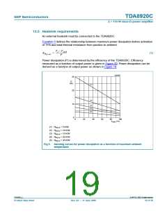
13.4 External clock
To ensure duty cycle-independent operation, the external clock frequency is divided by
two internally. The external clock frequency is therefore twice the internal clock frequency
(typically 2 × 350 kHz = 700 kHz).
If several class-D amplifiers are used in a single application, it is recommended that all the
devices run at the same switching frequency. This can be achieved by connecting the
OSC pins together and feeding them from an external oscillator. When using an external
oscillator, it is necessary to force pin OSC to a DC level above SGND. This disables the
internal oscillator and causes the PWM to switch at half the external clock frequency.
The internal oscillator requires an external resistor ROSC, connected between pin OSC
and pin VSSA. ROSC must be removed when using an external oscillator.
The noise generated by the internal oscillator is supply voltage dependent. An external
low-noise oscillator is recommended for low-noise applications running at high supply
voltages.
TDA8920C_2
© NXP B.V. 2009. All rights reserved.
Product data sheet
Rev. 02 — 11 June 2009
18 of 39

 NXP [ NXP ]