TDA8920C
NXP Semiconductors
2 × 110 W class-D power amplifier
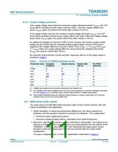
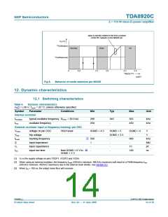
slope is directly related to the time-constant
of the RC network on the MODE pin
V
(V)
O
V
O(offset)(on)
Standby
Mute
On
V
O(offset)(mute)
0
0.8
2.2
3.0
4.2
5.5
V
(V)
MODE
coa021
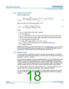
Fig 8.
Behavior of mode selection pin MODE
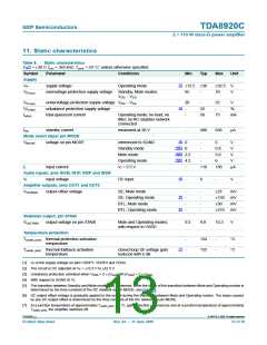
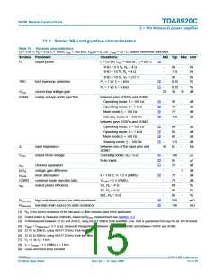
12. Dynamic characteristics
12.1 Switching characteristics
Table 9.
Dynamic characteristics
VP[1] = ±30 V; Tamb = 25 °C; unless otherwise specified.
Symbol Parameter Conditions
Internal oscillator
Min
Typ
Max
Unit
fosc(typ)
fosc
typical oscillator frequency ROSC = 30.0 kΩ
290
250
345
-
365
450
kHz
kHz
oscillator frequency
External oscillator input or frequency tracking; pin OSC
VOSC
Vtrip
ftrack
Zi
voltage on pin OSC
trip voltage
HIGH-level
SGND + 4.5
SGND + 5
SGND + 6
V
-
SGND + 2.5
-
V
[2]
tracking frequency
input impedance
input capacitance
input rise time
500
-
-
-
-
900
-
kHz
MΩ
pF
ns
1
-
Ci
15
100
[3]
tr(i)
from SGND + 0 V to
SGND + 5 V
-
[1] VP is the supply voltage on pins VDDP1, VDDP2 and VDDA.
[2] When using an external oscillator, the frequency ftrack (500 kHz minimum, 900 kHz maximum) will result in a PWM frequency fosc
(250 kHz minimum, 450 kHz maximum) due to the internal clock divider; see Section 8.2.
[3] When tr(i) > 100 ns, the output noise floor will increase.
TDA8920C_2
© NXP B.V. 2009. All rights reserved.
Product data sheet
Rev. 02 — 11 June 2009
14 of 39

 NXP [ NXP ]