TDA8920C
NXP Semiconductors
2 × 110 W class-D power amplifier
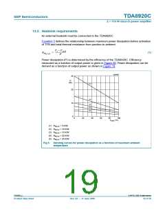
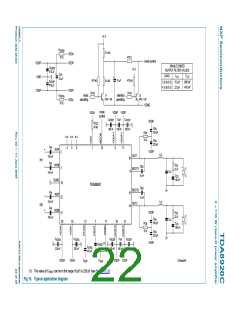
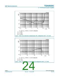
In the following example, a heatsink calculation is made for an 8 Ω BTL application with a
±30 V supply:
The audio signal has a crest factor of 10 (the ratio between peak power and average
power (20 dB)); this means that the average output power is 1⁄10 of the peak power.
Thus, the peak RMS output power level is the 0.5 % THD level, i.e. 170 W.
The average power is then 1⁄10 × 170 W = 17 W.
The dissipated power at an output power of 17 W is approximately 7 W.
When the maximum expected ambient temperature is 50 °C, the total Rth(j-a) becomes
(148 – 50)
= 14 K/W
-------------------------
7
Rth(j-a) = Rth(j-c) + Rth(c-h) + Rth(h-a)
Rth(j-c) (thermal resistance from junction to case) = 1.1 K/W
Rth(c-h) (thermal resistance from case to heatsink) = 0.5 K/W to 1 K/W (dependent on
mounting)
So the thermal resistance between heatsink and ambient temperature is:
Rth(h-a) (thermal resistance from heatsink to ambient) = 14 − (1.1 + 1) = 11.9 K/W
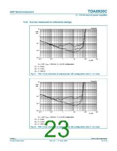
The derating curves for power dissipation (for several Rth(j-a) values) are illustrated in
Figure 9. A maximum junction temperature Tj = 150 °C is taken into account. The
maximum allowable power dissipation for a given heatsink size can be derived, or the
required heatsink size can be determined, at a required power dissipation level; see
Figure 9.
13.6 Pumping effects
In a typical stereo single-ended configuration, the TDA8920C is supplied by a symmetrical
supply voltage (e.g. VDD = 30 V and VSS = −30 V). When the amplifier is used in an SE
configuration, a ‘pumping effect’ can occur. During one switching interval, energy is taken
from one supply (e.g. VDD), while a part of that energy is returned to the other supply line
(e.g. VSS) and vice versa. When the voltage supply source cannot sink energy, the voltage
across the output capacitors of that voltage supply source increases and the supply
voltage is pumped to higher levels. The voltage increase caused by the pumping effect
depends on:
• Speaker impedance
• Supply voltage
• Audio signal frequency
• Value of supply line decoupling capacitors
• Source and sink currents of other channels
Pumping effects should be minimized to prevent the malfunctioning of the audio amplifier
and/or the voltage supply source. Amplifier malfunction due to the pumping effect can
trigger UVP, OVP or UBP.
TDA8920C_2
© NXP B.V. 2009. All rights reserved.
Product data sheet
Rev. 02 — 11 June 2009
20 of 39

 NXP [ NXP ]