LPC546xx
NXP Semiconductors
32-bit ARM Cortex-M4 microcontroller
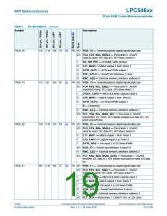
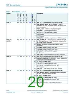
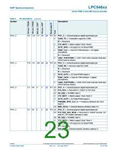
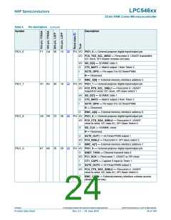
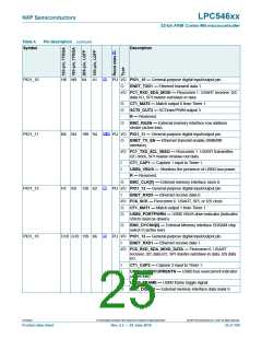
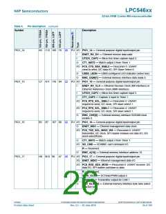
Table 4.
Symbol
Pin description …continued
Description
[2]
PIO1_2
G9 L14 117 58
PU I/O PIO1_2 — General-purpose digital input/output pin.
O
CAN0_TD — Transmitter output for CAN0.
R — Reserved.
O
I
CT0_MAT3 — Match output 3 from Timer0.
SCT0_GPI6 — Pin input 6 to SCTimer/PWM.
O
PDM1_CLK — Clock for PDM interface 1, for digital
microphone.
R — Reserved.
O
USB1_PORTPWRN — USB1 VBUS drive indicator (Indicates
VBUS must be driven).
[2]
PIO1_3
F10 J13 120 60
PU I/O PIO1_3 — General-purpose digital input/output pin.
I
CAN0_RD — Receiver input for CAN0.
R — Reserved.
R — Reserved.
O
I
SCT0_OUT4 — SCTimer/PWM output 4.
PDM1_DATA — Data for PDM interface 1 (digital
microphone).
O
USB0_PORTPWRN — USB0 VBUS drive indicator (Indicates
VBUS must be driven).
[2]
PIO1_4
C3 D4
3
3
PU I/O PIO1_4 — General-purpose digital input/output pin.
I/O FC0_SCK — Flexcomm 0: USART or SPI clock.
I/O SD_D[0] — SD/MMC data 0.
O
O
I
CT2_MAT1 — Match output 1 from Timer 2.
SCT0_OUT0 — SCTimer/PWM output 0.
FREQME_GPIO_CLK_A — Frequency Measure pin clock
input A.
I/O EMC_D[11]) — External Memory interface data [11].
PU I/O PIO1_5 — General-purpose digital input/output pin.
[2]
PIO1_5
C2 E4
5
4
I/O FC0_RXD_SDA_MOSI — Flexcomm 0: USART receiver, I2C
data I/O, SPI master-out/slave-in data.
I/O SD_D[2] — SD/MMC data 2.
O
I
CT2_MAT0 — Match output 0 from Timer 2.
SCT0_GPI0 — Pin input 0 to SCTimer/PWM.
R — Reserved.
O
EMC_A[4] — External memory interface address 4.
LPC546xx
All information provided in this document is subject to legal disclaimers.
© NXP Semiconductors N.V. 2018. All rights reserved.
Product data sheet
Rev. 2.5 — 20 June 2018
23 of 169

 NXP [ NXP ]