LPC546xx
NXP Semiconductors
32-bit ARM Cortex-M4 microcontroller
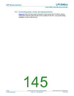
3.3 V
3.3 V
3.3 V
SWD connector
(4)
~10 kΩ - 100 kΩ
(6)
XTALIN
SWDIO/PIO0_12
C1
C2
1
2
(1)
XTALOUT
RTCXIN
DGND
~10 kΩ - 100 kΩ
SWCLK/PIO0_11
(6)
3
4
n.c.
n.c.
C3
C4
6
8
5
7
9
(1)
n.c.
RTCXOUT
DGND
RESETN
10
V
SS
(2)
V
DD
3.3 V
0.1 ꢀF
0.01 ꢀF
DGND
DGND
V
SSA
DGND
DGND
LPC546xx
AGND
PIO0_4
(3)
V
DDA
3.3 V
0.1 ꢀF
10 ꢀF
PIO0_5
PIO0_6
ISP select pins
(3)
VREFP
ADCx
3.3 V
(5)
0.1 ꢀF
10 ꢀF
0.1 ꢀF
VREFN
AGND
AGND
(7)
VBAT
3.3 V
0.1 ꢀF
AGND
DGND
DGND
aaa-026743
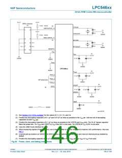
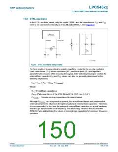
(1) See Section 13.6 “XTAL oscillator” for the values of C1, C2, C3, and C4.
(2) Position the decoupling capacitors of 0.1 μF and 0.01 μF as close as possible to the VDD pin. Add one set of decoupling
capacitors to each VDD pin.
(3) Position the decoupling capacitors of 0.1 μF as close as possible to the VREFN and VDDA pins. The 10 μF bypass capacitor
filters the power line. Tie VDDA and VREFP to VDD if the ADC is not used. Tie VREFN to VSS if ADC is not used.
(4) Uses the ARM 10-pin interface for SWD.
(5) When measuring signals of low frequency, use a low-pass filter to remove noise and to improve ADC performance. Also see
Ref. 3.
(6) External pull-up resistors on SWDIO and SWCLK pins are optional because these pins have an internal pull-up enabled by
default.
(7) Position the decoupling capacitor of 0.1 F as close as possible to the VBAT pin. Tie VBAT to VDD if not used.
Fig 45. Power, clock, and debug connections
LPC546xx
All information provided in this document is subject to legal disclaimers.
© NXP Semiconductors N.V. 2018. All rights reserved.
Product data sheet
Rev. 2.5 — 20 June 2018
146 of 169

 NXP [ NXP ]