74HC165; 74HCT165
NXP Semiconductors
8-bit parallel-in/serial out shift register
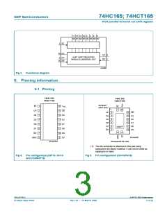
6.2 Pin description
Table 2.
Symbol
PL
Pin description
Pin
Description
1
asynchronous parallel load input (active LOW)
clock input (LOW-to-HIGH edge-triggered)
complementary output from the last stage
ground (0 V)
CP
2
Q7
7
GND
Q7
8
9
serial output from the last stage
serial data input
DS
10
D0 to D7
CE
11, 12, 13, 14, 3, 4, 5, 6
parallel data inputs (also referred to as Dn)
clock enable input (active LOW)
positive supply voltage
15
16
VCC
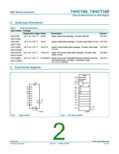
7. Functional description
Table 3.
Function table[1]
Operating modes Inputs
PL
Qn registers
Outputs
CE
X
X
L
CP
X
X
↑
DS
X
X
l
D0 to D7 Q0
Q1 to Q6 Q7
Q7
H
parallel load
L
L
L
L to L
L
L
H
X
X
X
X
X
X
H
L
H to H
H
L
serial shift
H
H
H
H
H
H
q0 to q5 q6
q0 to q5 q6
q0 to q5 q6
q0 to q5 q6
q1 to q6 q7
q1 to q6 q7
q6
q6
q6
q6
q7
q7
L
↑
h
H
L
↑
L
l
↑
L
h
H
q0
q0
hold “do nothing”
H
X
X
H
X
X
[1] H = HIGH voltage level;
h = HIGH voltage level one set-up time prior to the LOW-to-HIGH clock transition;
L = LOW voltage level;
l = LOW voltage level one set-up time prior to the LOW-to-HIGH clock transition;
q = state of the referenced output one set-up time prior to the LOW-to-HIGH clock transition;
X = don’t care;
↑ = LOW-to-HIGH clock transition.
74HC_HCT165_3
© NXP B.V. 2008. All rights reserved.
Product data sheet
Rev. 03 — 14 March 2008
4 of 22

 NXP [ NXP ]