74HC165; 74HCT165
NXP Semiconductors
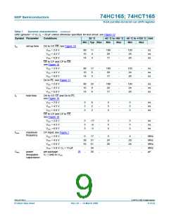
8-bit parallel-in/serial out shift register
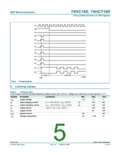
11 12 13 14 3
4
5
6
D0 D1 D2 D3 D4 D5 D6 D7
1
PL
10 DS
Q7
Q7
9
7
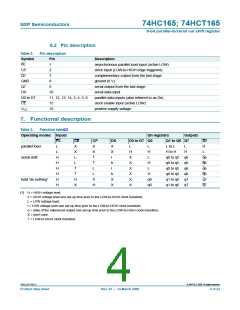
8-BIT SHIFT REGISTER
PARALLEL-IN/SERIAL-OUT
2
CP
15 CE
mna992
Fig 3. Functional diagram
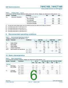
6. Pinning information
6.1 Pinning
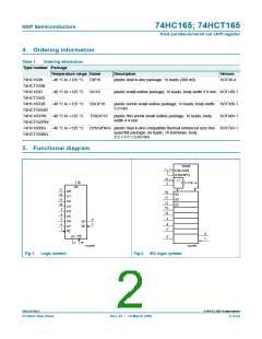
74HC165
74HCT165
74HC165
74HCT165
terminal 1
index area
1
2
3
4
5
6
7
8
16
15
14
13
12
11
10
9
PL
CP
V
CC
CE
D3
D2
D1
D0
DS
Q7
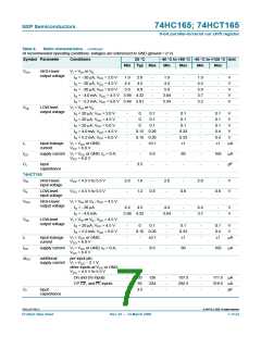
2
3
4
5
6
7
15
14
13
12
11
10
CP
CE
D3
D2
D1
D0
DS
D4
D4
D5
D6
D7
Q7
D5
D6
(1)
GND
D7
Q7
001aah565
GND
Transparent top view
001aah564
(1) The die substrate is attached to this pad using
conductive die attach material. It can not be used as
supply pin or input.
Fig 4. Pin configuration (DIP16, SO16
and (T)SSOP16)
Fig 5. Pin configuration (DHVQFN16)
74HC_HCT165_3
© NXP B.V. 2008. All rights reserved.
Product data sheet
Rev. 03 — 14 March 2008
3 of 22

 NXP [ NXP ]