M25PX64
Power-up and power-down
7
Power-up and power-down
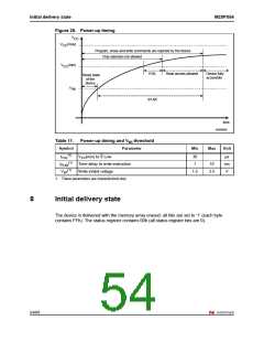
At power-up and power-down, the device must not be selected (that is Chip Select (S) must
follow the voltage applied on VCC) until VCC reaches the correct value:
V
CC(min) at power-up, and then for a further delay of tVSL
VSS at power-down.
A safe configuration is provided in Section 3: SPI modes.
To avoid data corruption and inadvertent write operations during power-up, a power on reset
(POR) circuit is included. The logic inside the device is held reset while VCC is less than the
power on reset (POR) threshold voltage, VWI – all operations are disabled, and the device
does not respond to any instruction.
Moreover, the device ignores all write enable (WREN), page program (PP), dual input fast
program (DIFP), program OTP (POTP), subsector erase (SSE), sector erase (SE), bulk
erase (BE), write status register (WRSR) and write to lock register (WRLR) instructions until
a time delay of tPUW has elapsed after the moment that VCC rises above the VWI threshold.
However, the correct operation of the device is not guaranteed if, by this time, VCC is still
below VCC(min). No write status register, program or erase instructions should be sent until
the later of:
tPUW after VCC has passed the VWI threshold
VSL after VCC has passed the VCC(min) level.
t
These values are specified in Table 11.
If the time, tVSL, has elapsed, after VCC rises above VCC(min), the device can be selected
for read instructions even if the tPUW delay has not yet fully elapsed.
After power-up, the device is in the following state:
The device is in the standby power mode (not the deep power-down mode)
The write enable latch (WEL) bit is reset
The write in progress (WIP) bit is reset
The lock registers are configured as: (write lock bit, lock down bit) = (0,0).
Normal precautions must be taken for supply line decoupling, to stabilize the VCC supply.
Each device in a system should have the VCC line decoupled by a suitable capacitor close
to the package pins (generally, this capacitor is of the order of 100 nF).
At power-down, when VCC drops from the operating voltage, to below the power on reset
(POR) threshold voltage, VWI, all operations are disabled and the device does not respond
to any instruction (the designer needs to be aware that if power-down occurs while a write,
program or erase cycle is in progress, some data corruption may result).
VPPH must be applied only when VCC is stable and in the VCC(min) to VCC(max)
voltage range.
53/68

 NUMONYX [ NUMONYX B.V ]