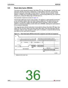
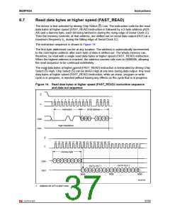
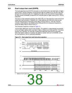
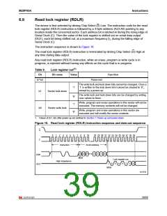
Instructions
M25PX64
6.10
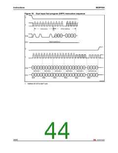
Read OTP (ROTP)
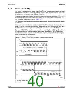
The device is first selected by driving Chip Select (S) Low. The instruction code for the read
OTP (ROTP) instruction is followed by a 3-byte address (A23- A0) and a dummy byte. Each
bit is latched in on the rising edge of Serial Clock (C).
Then the memory contents at that address are shifted out on serial data output (DQ1). Each
bit is shifted out at the maximum frequency, fCmax, on the falling edge of Serial Clock (C).
The instruction sequence is shown in Figure 17.
The address is automatically incremented to the next higher address after each byte of data
is shifted out.
There is no rollover mechanism with the read OTP (ROTP) instruction. This means that the
read OTP (ROTP) instruction must be sent with a maximum of 65 bytes to read, since once
the 65th byte has been read, the same (65th) byte keeps being read on the DQ1 pin.
The read OTP (ROTP) instruction is terminated by driving Chip Select (S) High. Chip Select
(S) can be driven High at any time during data output. Any read OTP (ROTP) instruction
issued while an erase, program or write cycle is in progress, is rejected without having any
effect on the cycle that is in progress.
Figure 17. Read OTP (ROTP) instruction and data-out sequence
S
0
1
2
3
4
5
6
7
8
9
10
28 29 30 31
C
Instruction
24-bit address
23 22 21
3
2
1
0
DQ0
DQ1
High Impedance
S
C
47
32 33 34 35 36 37 38 39 40 41 42 43 44 45 46
Dummy byte
7
6
5
4
3
2
0
1
DQ0
DQ1
DATA OUT n
DATA OUT 1
7
6
5
4
3
2
1
0
7
7
6
5
4
3
2
0
1
MSB
MSB
MSB
AI13573
1. A23 to A7 are don't care.
2. 1 ≤ n ≤ 65.
40/68

 NUMONYX [ NUMONYX B.V ]