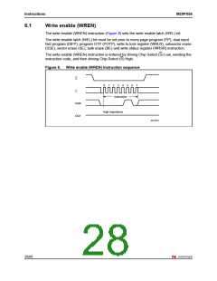
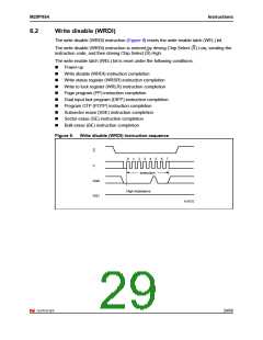
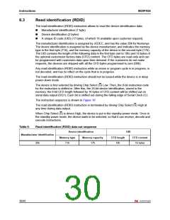
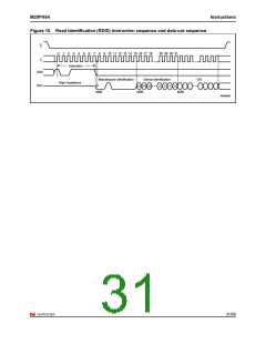
Instructions
M25PX64
6.4
Read status register (RDSR)
The read status register (RDSR) instruction allows the status register to be read. The status
register may be read at any time, even while a program, erase or write status register cycle
is in progress. When one of these cycles is in progress, it is recommended to check the
write in progress (WIP) bit before sending a new instruction to the device. It is also possible
to read the status register continuously, as shown in Figure 11.
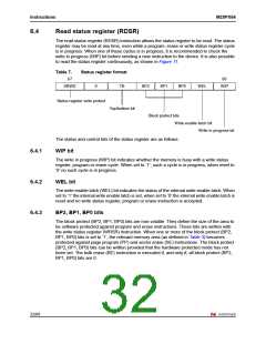
Table 7.
Status register format
b7
b0
SRWD
0
TB
BP2
BP1
BP0
WEL
WIP
Status register write protect
Top/bottom bit
Block protect bits
Write enable latch bit
Write in progress bit
The status and control bits of the status register are as follows:
6.4.1
6.4.2
6.4.3
WIP bit
The write in progress (WIP) bit indicates whether the memory is busy with a write status
register, program or erase cycle. When set to ‘1’, such a cycle is in progress, when reset to
‘0’ no such cycle is in progress.
WEL bit
The write enable latch (WEL) bit indicates the status of the internal write enable latch. When
set to ‘1’ the internal write enable latch is set, when set to ‘0’ the internal write enable latch is
reset and no write status register, program or erase instruction is accepted.
BP2, BP1, BP0 bits
The block protect (BP2, BP1, BP0) bits are non-volatile. They define the size of the area to
be software protected against program and erase instructions. These bits are written with
the write status register (WRSR) instruction. When one or more of the block protect (BP2,
BP1, BP0) bits is set to ‘1’, the relevant memory area (as defined in Table 3) becomes
protected against page program (PP) and sector erase (SE) instructions. The block protect
(BP2, BP1, BP0) bits can be written provided that the hardware protected mode has not
been set. The bulk erase (BE) instruction is executed if, and only if, all block protect (BP2,
BP1, BP0) bits are 0.
32/68

 NUMONYX [ NUMONYX B.V ]