Instructions
M25PX64
6.5
Write status register (WRSR)
The write status register (WRSR) instruction allows new values to be written to the status
register. Before it can be accepted, a write enable (WREN) instruction must previously have
been executed. After the write enable (WREN) instruction has been decoded and executed,
the device sets the write enable latch (WEL).
The write status register (WRSR) instruction is entered by driving Chip Select (S) Low,
followed by the instruction code and the data byte on serial data input (DQ0).
The instruction sequence is shown in Figure 12.
The write status register (WRSR) instruction has no effect on b6, b1 and b0 of the status
register. b6 is always read as ‘0’.
Chip Select (S) must be driven High after the eighth bit of the data byte has been latched in.
If not, the write status register (WRSR) instruction is not executed. As soon as Chip Select
(S) is driven High, the self-timed write status register cycle (whose duration is tW) is initiated.
While the write status register cycle is in progress, the status register may still be read to
check the value of the write in progress (WIP) bit. The write in progress (WIP) bit is 1 during
the self-timed write status register cycle, and is 0 when it is completed. When the cycle is
completed, the write enable latch (WEL) is reset.
The write status register (WRSR) instruction allows the user to change the values of the
block protect (BP2, BP1, BP0) bits, to define the size of the area that is to be treated as
read-only, as defined in Table 3. The write status register (WRSR) instruction also allows the
user to set and reset the status register write disable (SRWD) bit in accordance with the
Write Protect (W/VPP) signal. The status register write disable (SRWD) bit and Write Protect
(W/VPP) signal allow the device to be put in the hardware protected mode (HPM). The write
status register (WRSR) instruction is not executed once the hardware protected mode
(HPM) is entered.
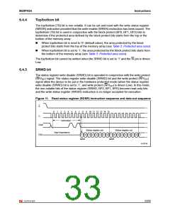
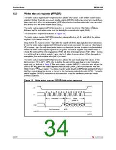
Figure 12. Write status register (WRSR) instruction sequence
S
0
1
2
3
4
5
6
7
8
9
10 11 12 13 14 15
C
Instruction
Status
register in
7
6
5
4
3
2
0
1
DQ0
DQ1
High Impedance
MSB
AI13735
34/68

 NUMONYX [ NUMONYX B.V ]