®
Numonyx™ StrataFlash Embedded Memory (J3-65nm)
1.0
Functional Overview
The Numonyx™ StrataFlash® Embedded Memory (J3-65nm) provides improved
mainstream performance with enhanced security features, taking advantage of the
high quality and reliability of the NOR-based Numonyx 65 nm ETOX™ X process technology.
Offered in 32-Mbit up through 256-Mbit densities, the Numonyx™ Embedded Memory
(J3-65nm) device brings reliable, low-voltage capability (3 V read, program, and
erase) with high speed, low-power operation. The Numonyx™ StrataFlash® Embedded
Memory (J3-65nm) device is ideal for code and data applications where high density
and low cost are required, such as in networking, telecommunications, digital set top
boxes, audio recording, and digital imaging. Numonyx Flash Memory components also
deliver a new generation of forward-compatible software support. By using the
Common Flash Interface (CFI) and Scalable Command Set (SCS), customers can take
advantage of density upgrades and optimized write capabilities of future Numonyx
Flash Memory devices.
1.1
Document purpose
This document contains information pertaining to the Numonyx™ StrataFlash®
Embedded Memory (J3-65nm) device features, operation, and specifications.
The Numonyx™ Embedded Memory (J3-65nm) device is offered in Single Bit Cell
technology for 32-, 64-, 128-Mbit densities. The Numonyx™ StrataFlash® Embedded
Memory (J3-65nm) device is offered in Multi-Level Cell technology for 256-Mbit density.
This document just covers 256-Mbit die information.
Unless otherwise indicated throughout the rest of this document, Numonyx™
StrataFlash® Embedded Memory (J3-65nm) is referred to as J3-65nm.
1.2
Product overview
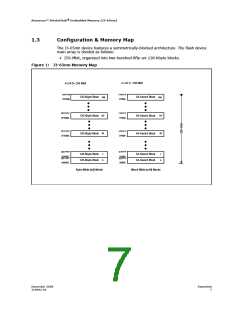
The 256-Mbit J3-65nm is organized as 256 individual 128Kbyte symmetrical blocks.
A 128-bit Protection Register has multiple uses, including unique flash device
identification.
The J3-65nm device includes new security features that were not available on the
(previous) 0.25µm, 0.18µm, and 0.13µm versions of the J3 family. The new security
features can be implemented to protect critical code and data from unwanted
modification (program or erase). Usage can be defined to fit the specific needs of each
customer.
The J3-65nm optimized architecture and interface dramatically increases read
performance by supporting page-mode reads. This read mode is ideal for non-clock
memory systems.
The J3-65nm Common Flash Interface (CFI) permits software algorithms to be used for
entire families of devices. This allows device-independent, JEDEC ID-independent, and
forward- and backward-compatible software support for the specified flash device
families. Flash vendors can standardize their existing interfaces for long-term
compatibility.
The Scalable Command Set (SCS) allows a single, simple software driver in all host
systems to work with all SCS-compliant flash memory devices, independent of system-
level packaging (e.g., memory card, SIMM, or direct-to-board placement). Additionally,
SCS provides the highest system/device data transfer rates and minimizes device and
system-level implementation costs.
December 2008
319942-02
Datasheet
5

 NUMONYX [ NUMONYX B.V ]