®
Numonyx™ StrataFlash Embedded Memory (J3-65nm)
Contents
1.0 Functional Overview..................................................................................................5
1.1
1.2
1.3
1.4
Document purpose ..............................................................................................5
Product overview.................................................................................................5
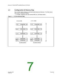
Configuration & Memory Map................................................................................7
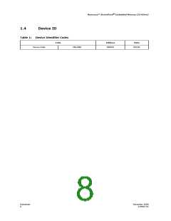
Device ID...........................................................................................................8
2.0 Package Information.................................................................................................9
2.1
2.2
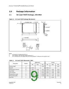
56-Lead TSOP Package, 256-Mbit..........................................................................9
Easy BGA Package, 256-Mbit .............................................................................. 11
3.0 Ballout..................................................................................................................... 12
3.1
3.2
Easy BGA Ballout, 256-Mbit ................................................................................ 12
56-Lead TSOP Package Pinout, 256-Mbit .............................................................. 13
4.0 Signal Descriptions.................................................................................................. 14
5.0 Bus Interface........................................................................................................... 15
5.1
5.2
5.3
5.4
5.5
Reads.............................................................................................................. 16
Writes.............................................................................................................. 16
Output Disable.................................................................................................. 16
Standby........................................................................................................... 16
Reset............................................................................................................... 17
6.0 Command Set .......................................................................................................... 18
6.1
6.2
Device Command Codes..................................................................................... 18
Device Command Bus Cycle................................................................................ 19
7.0 Read operation........................................................................................................ 21
7.1
7.2
7.3
7.4
7.5
Read Array....................................................................................................... 21
Asynchronous Page Mode Read ........................................................................... 21
Read Status Register ......................................................................................... 22
Read Device Information.................................................................................... 22
CFI Query ........................................................................................................ 22
8.0 Program operation .................................................................................................. 24
8.1
8.2
8.3
Single-Word/Byte Programming .......................................................................... 24
Buffered Programming....................................................................................... 24
Suspend/Resume .............................................................................................. 25
9.0 Erase Operation....................................................................................................... 26
9.1
9.2
Block Erase ...................................................................................................... 26
Suspend/Resume .............................................................................................. 26
10.0 Security................................................................................................................... 28
10.1 Normal Block Locking......................................................................................... 28
10.2 Configurable Block Locking ................................................................................. 28
10.3 VPEN Protection ................................................................................................ 29
10.4 Password Access ............................................................................................... 29
11.0 Registers................................................................................................................. 30
11.1 Status Register ................................................................................................. 30
11.2 Status Signal.................................................................................................... 31
11.3 OTP Protection Register...................................................................................... 32
12.0 Power and Reset Specifications............................................................................... 35
12.1 Power-Up and Power-Down................................................................................. 35
December 2008
319942-02
Datasheet
3

 NUMONYX [ NUMONYX B.V ]