DC and AC Parameters
M29FxxxFT, M29FxxxFB
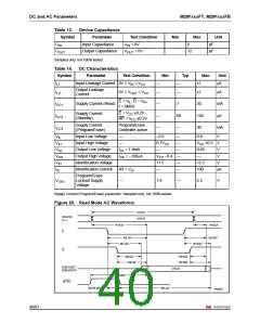
Table 13. Device Capacitance
Symbol
CIN
COUT
Parameter
Test Condition
VIN = 0V
Min
Max
Unit
Input Capacitance
Output Capacitance
6
pF
pF
VOUT = 0V
12
Sampled only, not 100% tested.
Table 14. DC Characteristics
Symbol
ILI
Parameter
Test Condition
Min
Typ
Max
Unit
Input Leakage Current 0V ≤ VIN ≤ VCC
—
—
—
±1
±1
µA
µA
Output Leakage
0V ≤ VOUT ≤ VCC
Current
ILO
—
7
E = VIL, G = VIH,
Supply Current (Read)
f = 6MHz
ICC1
ICC2
ICC3
—
—
—
20
mA
µA
E = VCC ±0.2V,
RP = VCC ±0.2V
Supply Current
(Standby)
60
—
120
30
0.8
Supply Current
(Program/Erase)
Program/Erase
Controller active
mA
VIL
Input Low Voltage
Input High Voltage
Output Low Voltage
Output High Voltage
Identification Voltage
Identification Current
—
–0.5
—
—
—
—
—
—
V
VIH
VOL
VOH
VID
IID
—
0.7VCC
—
VCC +0.3
0.45
—
V
IOL = 1.8mA
IOH = –100µA
V
VCC –0.4
11.5
V
12.5
100
V
A9 = VID
—
—
µA
Program/Erase
Lockout Supply
Voltage
VLKO
1.8
—
2.3
V
Supply Current (Program/Erase) parameter: Sampled only, not 100% tested.
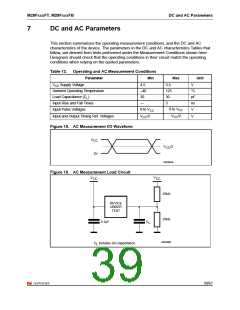
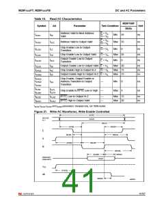
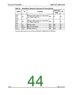
Figure 20. Read Mode AC Waveforms
tAVAV
A0-A19/
VALID
A–1
tAVQV
tAXQX
E
tELQV
tEHQX
tELQX
tEHQZ
G
tGLQX
tGLQV
tGHQX
tGHQZ
DQ0-DQ7/
DQ8-DQ15
VALID
tBHQV
BYTE
tELBL/tELBH
tBLQZ
AI02922
40/67

 NUMONYX [ NUMONYX B.V ]