Signal Descriptions
M29FxxxFT, M29FxxxFB
2
Signal Descriptions
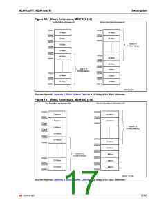
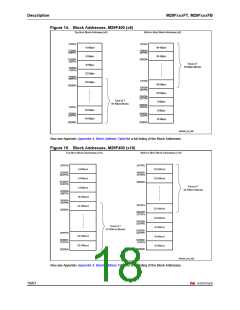
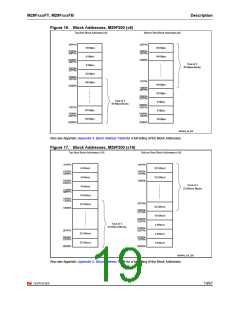
See Figure 1.: Logic Diagram and Table 1.: Signal Names, for a brief overview of the signals
connected to this device.
2.1
2.2
2.3
Address Inputs (A0-A19)
The Address Inputs select the cells in the memory array to access during Bus Read
operations. During Bus Write operations they control the commands sent to the Command
Interface of the Program/Erase Controller.
Data Inputs/Outputs (DQ0-DQ7)
The Data Inputs/Outputs output the data stored at the selected address during a Bus Read
operation. During Bus Write operations they represent the commands sent to the Command
Interface of the Program/Erase Controller.
Data Inputs/Outputs (DQ8-DQ14)
The Data Inputs/Outputs output the data stored at the selected address during a Bus Read
operation when BYTE is High, V . When BYTE is Low, V , these pins are not used and are
IH
IL
high impedance. During Bus Write operations the Command Register does not use these
bits. When reading the Status Register these bits should be ignored.
2.4
Data Input/Output or Address Input (DQ15A-1)
When BYTE is High, V , this pin behaves as a Data Input/Output pin (as DQ8-DQ14).
IH
When BYTE is Low, V , this pin behaves as an address pin; DQ15A–1 Low will select the
IL
LSB of the Word on the other addresses, DQ15A–1 High will select the MSB. Throughout
the text consider references to the Data Input/Output to include this pin when BYTE is High
and references to the Address Inputs to include this pin when BYTE is Low except when
stated explicitly otherwise.
2.5
2.6
Chip Enable
The Chip Enable, E, activates the memory, allowing Bus Read and Bus Write operations to
be performed. When Chip Enable is High, V , all other pins are ignored.
IH
Output Enable
The Output Enable, G, controls the Bus Read operation of the memory.
20/67

 NUMONYX [ NUMONYX B.V ]