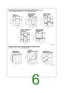
Application Information (Continued)
COMPARATORS
It is often a good idea to decrease the amount of hysteresis
until oscillations are observed, then use three times that
minimum hysteresis in the final circuit. Note that the amount
of hysteresis needed is greatly affected by layout. The
amount of hysteresis should be rechecked each time the
layout is changed, such as changing from a breadboard to a
P.C. board.
Any of the comparators or the reference may be biased in
any way with no effect on the other sections of the LM615,
except when a substrate diode conducts (see Electrical
Characteristics Note 3). For example, one or both inputs of
one comparator may be outside the input voltage range lim-
its, the reference may be unpowered, and the other compar-
ators will still operate correctly. Unused comparators should
have inverting input and output tied to Vb, and non-inverting
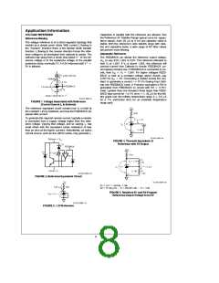
Input Stage
The input stage uses lateral PNP input transistors which,
unlike those of many op amps, have breakdown voltage
input tied to Va
.
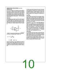
Hysteresis
BV
equal to the absolute maximum supply voltage. Also,
EBO
they have no diode clamps to the positive supply nor across
the inputs. These features make the inputs look like high
impedances to input sources producing large differential
and common-mode voltages.
Any comparator may oscillate or produce a noisy output if
the applied differential input voltage is near the compara-
tor’s offset voltage. This usually happens when the input
signal is moving very slowly across the comparator’s switch-
ing threshold. This problem can be prevented by the addi-
tion of hysteresis, or positive feedback, as shown in Figure
12.
The guaranteed common-mode input voltage range for an
LM615 is Vb
s
s
b
1.8V), over temperature.
V
CM
(Va
This is the voltage range in which the comparisons must be
made. If both inputs are within this range, the output will be
at the correct state. If one input is within this range, and the
other input is less than (Vb
32V), even if this is greater
a
than Va, the output will be at the correct state. If, however,
either or both inputs are driven below Vb, and either input
current exceeds 10 mA, the output state is not guaranteed
to be correct. If both inputs are above (Va
b
output state is also not guaranteed to be correct.
1.8V), the
Output Stage
TL/H/11057–20
The comparators have open-collector output stages which
require a pull-up resistor from each output pin to a positive
supply voltage of the output to switch properly. When the
internal output transistor is off, the output (HIGH) voltage
will be pulled up to this external positive voltage.
FIGURE 12. R and R Add Hysteresis to Comparator
F
S
The amount of hysteresis added in Figure 12 is
R
S
a
e
To ensure that the LOW output voltage is under the TTL-low
threshold, the output transistor’s load current must be less
than 0.8 mA (over temperature) when it turns on. This im-
pacts the minimum value of the pull-up resistor.
V
H
V
x
a
(R
R )
S
F
R
R
S
a
&
n
V
x
for R
R
S
F
F
A good rule of thumb is to add hysteresis of at least the
maximum specified offset voltage. More than about 50 mV
of hysteresis can substantially reduce the accuracy of the
comparator, since the offset voltage is effectively being in-
creased by the hysteresis when the comparator output is
high.
10

 NSC [ National Semiconductor ]