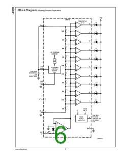
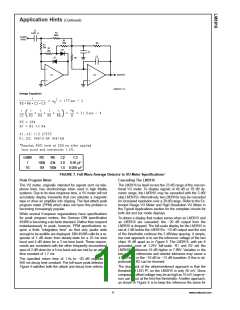
Functional Description
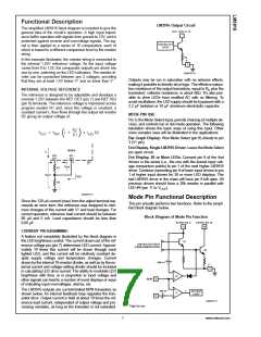
LM3916 Output Circuit
The simplified LM3916 block diagram is included to give the
general idea of the circuit’s operation. A high input imped-
ance buffer operates with signals from ground to 12V, and is
protected against reverse and overvoltage signals. The sig-
nal is then applied to a series of 10 comparators; each of
which is biased to a different comparison level by the resistor
string.
In the example illustrated, the resistor string is connected to
the internal 1.25V reference voltage. As the input voltage
varies from 0 to 1.25, the comparator outputs are driven low
one by one, switching on the LED indicators. The resistor di-
vider can be connected between any 2 voltages, providing
that they are at least 1.5V below V+ and no lower than V−.
DS007971-6
Outputs may be run in saturation with no adverse effects,
making it possible to directly drive logic. The effective satura-
tion resistance of the output transistors, equal to RE plus the
transistors’ collector resistance, is about 50Ω. It’s also pos-
sible to drive LEDs from rectified AC with no filtering. To
avoid oscillations, the LED supply should be bypassed with a
2.2 µF tantalum or 10 µF aluminum electrolytic capacitor.
INTERNAL VOLTAGE REFERENCE
The reference is designed to be adjustable and develops a
nominal 1.25V between the REF OUT (pin 7) and REF ADJ
(pin 8) terminals. The reference voltage is impressed across
program resistor R1 and, since the voltage is constant, a
constant current I1 then flows through the output set resistor
R2 giving an output voltage of:
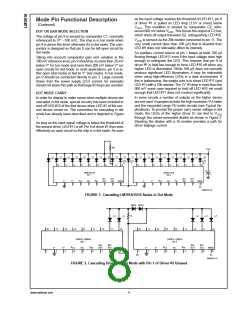
MODE PIN USE
Pin 9, the Mode Select input, permits chaining of multiple de-
vices, and controls bar or dot mode operation. The following
tabulation shows the basic ways of using this input. Other
more complex uses will be illustrated in the applications.
Bar Graph Display: Wire Mode Select (pin 9) directly to pin
3 (V+ pin).
Dot Display, Single LM3916 Driver: Leave the Mode Select
pin open circuit.
Dot Display, 20 or More LEDs: Connect pin 9 of the first
drivers in the series (i.e., the one with the lowest input volt-
age comparison points) to pin 1 of the next higher LM3916
driver. Continue connecting pin 9 of lower input drivers to pin
1 of higher input drivers for 30 or more LED displays. The
last LM3916 driver in the chain will have pin 9 left open. All
previous drivers should have a 20k resistor in parallel with
LED #9 (pin 11 to VLED).
DS007971-5
Mode Pin Functional Description
This pin actually performs two functions. Refer to the simpli-
fied block diagram below.
Since the 120 µA current (max) from the adjust terminal rep-
resents an error term, the reference was designed to mini-
mize changes of this current with V+ and load changes. For
correct operation, reference load current should be between
80 µA and 5 mA. Load capacitance should be less than
0.05 µF.
Block Diagram of Mode Pin Function
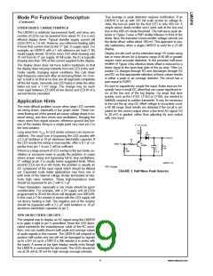
CURRENT PROGRAMMING
A feature not completely illustrated by the block diagram is
the LED brightness control. The current drawn out of the ref-
erence voltage pin (pin 7) determines LED current. Approxi-
mately 10 times this current will be drawn through each
lighted LED, and this current will be relatively constant de-
spite supply voltage and temperature changes. Current
drawn by the internal 10-resistor divider, as well as by the ex-
ternal current and voltage-setting divider should be included
in calculating LED drive current. The ability to modulate LED
brightness with time, or in proportion to input voltage and
other signals can lead to a number of novel displays or ways
of indicating input overvoltages, alarms, etc.
The LM3916 outputs are current-limited NPN transistors as
shown below. An internal feedback loop regulates the tran-
sistor drive. Output current is held at about 10 times the ref-
erence load current, independent of output voltage and pro-
cessing variables, as long as the transistor is not saturated.
DS007971-7
*
High for bar
7
www.national.com

 NSC [ National Semiconductor ]