Application Hints (Continued)
is open. If pins 2 and 6 are bypassed then R as low as 2 kX
can be used. This restriction is because the amplifier is only
compensated for closed-loop gains greater than 9 V/V.
beta is the value required for the current in R1 and R2:
b
(V /2)
S
V
BE
a
e
b
(R1
R2)
O
I
O MAX
0.7V and b
INPUT BIASING
e
e
100.
Good design values are V
BE
O
The schematic shows that both inputs are biased to ground
with a 50 kX resistor . The base current of the input transis-
tors is about 250 nA, so the inputs are at about 12.5 mV
when left open. If the dc source resistance driving the
LM388 is higher than 250 kX it will contribute very little
additional offset (about 2.5 mV at the input, 50 mV at the
output). If the dc source resistance is less than 10 kX, then
shorting the unused input to ground will keep the offset low
(about 2.5 mV at the input, 50 mV at the output). For dc
source resistances between these values we can eliminate
excess offset by putting a resistor from the unused input to
ground, equal in value to the dc source resistance. Of
course all offset problems are eliminated if the input is ca-
pacitively coupled.
e
Example: 1 watt into 8X load with V
12V.
e
500 mA
S
2 P
R
O
e
I
O MAX
0
L
b
(12/2) 0.7
0.5
a
e
e
1060X
(R1
R2)
100
#
J
To keep the current in R2 constant during positive swing
capacitor C is added. As the output swings positive C lifts
B
B
R1 and R2 above the supply, maintaining a constant voltage
e
across R2. To minimize the value of C , R1
B
due to C and R1 and R2 is usually set equal to the pole
B
due to the output coupling capacitor and the load. This
gives:
R2. The pole
When using the LM388 with higher gains (bypassing the
1.35 kX resistor between pins 2 and 6) it is necessary to
bypass the unused input, preventing degradation of gain
and possible instabilities. This is done with a 0.1 mF capaci-
tor or a short to ground depending on the dc source resist-
ance on the driven input.
4C
C
c
c
j
j
C
B
b
25
O
e
e
c
Example: for 100 Hz pole and R
e
8X; C
200 mF and
L
C
8 mF, if R1 is made a diode and R2 increased to give
B
the same current, C can be decreased by about a factor of
B
4, as in Figure 4.
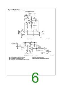
BOOTSTRAPPING
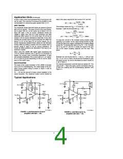
For reduced component count the load can replace R1. The
a
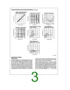
The base of the output transistor of the LM388 is brought
out to pin 9 for Bootstrapping. The output stage of the am-
plifier during positive swing is shown in Figure 3 with its
external circuitry.
value of (R1
R2) is the same, so R2 is increased. Now C
B
is both the coupling and the bootstrapping capacitor (see
Figure 2 ).
a
output transistor. The maximum output current divided by
R1
R2 set the amount of base current available to the
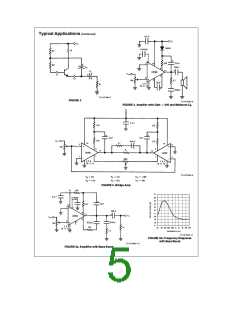
Typical Applications
TL/H/7846–3
TL/H/7846–4
FIGURE 1. Load Returned to Ground
e
FIGURE 2. Load Returned to V
e
(Amplifier with Gain 20)
S
(Amplifier with Gain
20)
4

 NSC [ National Semiconductor ]