Absolute Maximum Ratings
If Military/Aerospace specified devices are required,
please contact the National Semiconductor Sales
Office/Distributors for availability and specifications.
a
0 C to 70 C
Operating Temperature
§
§
Junction Temperature
150 C
§
Lead Temperature (Soldering, 10 sec.)
Thermal Resistance
260 C
§
Supply Voltage
15V
Package Dissipation 14-Pin DIP (Note 1)
Input Voltage
8.3W
i
i
30 C/W
§
JC
g
0.4V
79 C/W
§
JA
b
a
65 C to 150 C
Storage Temperature
§
§
e
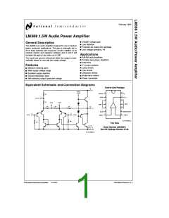
Electrical Characteristics T
25 C,(Figure 1)
§
A
Symbol
Parameter
Conditions
Min
Typ
Max
Units
V
S
Operating Supply Voltage
LM388
4
12
V
e
e
I
Quiescent Current
LM388
V
0
Q
IN
16
23
mA
V
S
12V
e
e
e
e
12V, R
e
180X, THD 10%
P
Output Power (Note 2)
LM388N-1
R1
R2
OUT
e
V
V
8X
1.5
0.6
2.2
0.8
W
W
S
L
e
6V, R
4X
S
L
e
e
1 kHz
A
Voltage Gain
V
12V, f
23
26
46
30
1
dB
dB
V
S
10 mF from Pins 2 to 6
e
e
BW
Bandwidth
V
S
12V, Pins 2 and 6 Open
300
0.1
kHz
%
e
e
500 mW,
THD
Total Harmonic Distortion
V
S
12V, R
8X, P
L
OUT
e
f
1 kHz, Pins 2 and 6 Open
e
e
Pins 2 and 6 Open, Referred to Output
e
10 mF,
PSRR
Power Supply Rejection Ratio
(Note 3)
V
S
12V, f
1 kHz, C
BYPASS
50
dB
R
Input Resistance
Input Bias Current
10
50
kX
IN
e
V
S
I
12V, Pins 7 and 8 Open
250
nA
BIAS
Note 1: Pins 3, 4, 5, 10, 11, 12 at 25 C. Derate at 15 C/W above 25 C case.
§
§
§
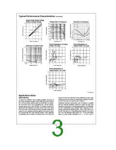
Note 2: The amplifier should be in high gain for full swing on higher supplies due to input voltage limitations.
Note 3: If load and bypass capacitor are returned to V (Figure 2), rather than ground (Figure 1), PSRR is typically 30 dB.
S
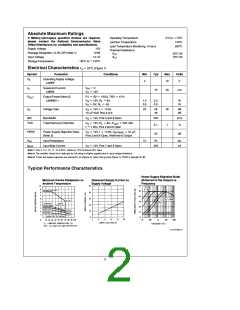
Typical Performance Characteristics
Power Supply Rejection Ratio
(Referred to the Output) vs
Frequency
Maximum Device Dissipation vs
Ambient Temperature
Quiescent Supply Current vs
Supply Voltage
TL/H/7846–5
2

 NSC [ National Semiconductor ]