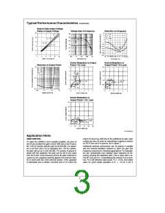
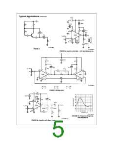
Typical Performance Characteristics (Continued)
Peak-to-Peak Output Voltage
Swing vs Supply Voltage
Voltage Gain vs Frequency
Distortion vs Frequency
Device Dissipation vs Output
PowerÐ4X Load
Device Dissipation vs
Output PowerÐ8X Load
Distortion vs Output Power
Device Dissipation vs
Output PowerÐ16X Load
TL/H/7846–6
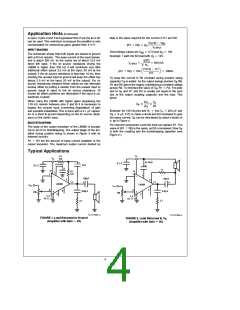
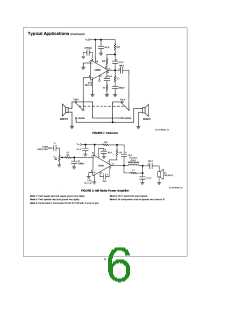
Application Hints
GAIN CONTROL
output dc level may shift due to the additional dc gain. Gain
control can also be done by capacitively coupling a resistor
(or FET) from pin 6 to ground, as in Figure 7.
To make the LM388 a more versatile amplifier, two pins (2
and 6) are provided for gain control. With pins 2 and 6 open,
the 1.35 kX resistor sets the gain at 20 (26 dB). If a capaci-
tor is put from pins 2 to 6, bypassing the 1.35 kX resistor,
the gain will go up to 200 (46 dB). If a resistor is placed in
series with the capacitor, the gain can be set to any value
from 20 to 200. A low frequency pole in the gain response is
caused by the capacitor working against the external resis-
tor in series with the 150X internal resistor. If the capacitor
is eliminated and a resistor connects pins 2 to 6 then the
Additional external components can be placed in parallel
with the internal feedback resistors to tailor the gain and
frequency response for individual applications. For example,
we can compensate poor speaker bass response by fre-
quency shaping the feedback path. This is done with a se-
ries RC from pin 6 to 13 (paralleling the internal 15 kX resis-
j
e
tor). For 6 dB effective bass boost: R
value for good stable operation is R
15 kX, the lowest
10 kX if pin 2
3

 NSC [ National Semiconductor ]