Current Limit Operation
Functional Description (Continued)
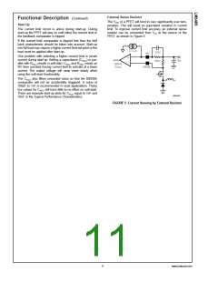
The LM3485 has a cycle-by-cycle current limit. Current limit
is sensed across the VDS of the PFET or across an addi-
tional sense resistor. When current limit is reached, the
LM3485 turns off the external PFET for a period of 9µs. The
The minimum output voltage ripple (VOUT_PP) can be calcu-
lated in the same way.
VOUT_PP = VHYST ( R1 + R2 ) / R2
current limit is adjusted by an external resistor, RADJ
.
For example, with VOUT set to 3.3V, VOUT_PP is 26.6mV
The current limit circuit is composed of the ISENSE com-
parator and the one-shot pulse generator. The positive input
of the ISENSE comparator is the ADJ pin. An internal 5.5µA
current sink creates a voltage across the external RADJ
resister. This voltage is compared to the voltage across the
PFET or sense resistor. The ADJ voltage can be calculated
as follows.
*
VOUT_PP = 0.01 ( 33K + 20K ) / 20K = 0.0266V
Operating frequency (F) is determined by knowing the input
voltage, output voltage, inductor, VHYST, ESR (Equivalent
Series Resistance) of output capacitor, and the delay. It can
be approximately calculated using the formula:
*
VADJ = VIN − (RADJ 5.5µA)
The negative input of the ISENSE comparator is the ISENSE
pin that should be connected to the drain of the external
PFET. The inductor current is determined by sensing the
where:
VDS. It can be calculated as follows.
α: ( R1 + R2 ) / R2
*
VISENSE = VIN − (RDSON IIND_PEAK) = VIN − VDS
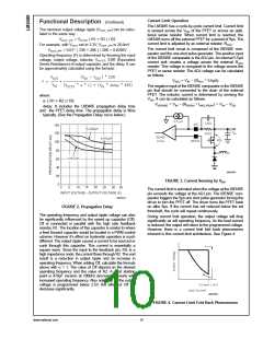
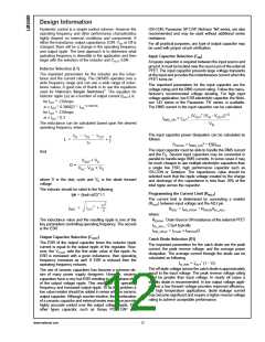
delay: It includes the LM3485 propagation delay time
and the PFET delay time. The propagation delay is 90ns
typically. (See the Propagation Delay curve below.)
20034625
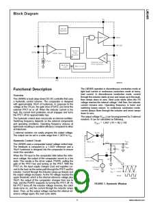
FIGURE 3. Current Sensing by VDS
The current limit is activated when the voltage at the ISENSE
pin exceeds the voltage at the ADJ pin. The ISENSE com-
parator triggers the 9µs one shot pulse generator forcing the
driver to turn the PFET off. The driver turns the PFET back
on after 9µs. If the current has not reduced below the set
threshold, the cycle will repeat continuously.
20034614
FIGURE 2. Propagation Delay
The operating frequency and output ripple voltage can also
be significantly influenced by the speed up capacitor (Cff).
Cff is connected in parallel with the high side feedback
resistor, R1. The location of this capacitor is similar to where
a feed forward capacitor would be located in a PWM control
scheme. However it’s effect on hysteretic operation is much
different. The output ripple causes a current to be sourced or
sunk through this capacitor. This current is essentially a
square wave. Since the input to the feedback pin, FB, is a
high impedance node, the current flows through R2. The end
result is a reduction in output ripple and an increase in
operating frequency. When adding Cff, calculate the formula
above with α = 1. The value of Cff depend on the desired
operating frequency and the value of R2. A good starting
point is 470pF ceramic at 100kHz decreasing linearly with
increased operating frequency. Also note that as the output
voltage is programmed below 2.5V, the effect of Cff will
decrease significantly.
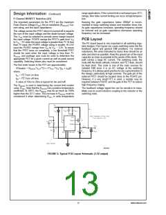
During current limit operation, the output voltage will drop
significantly as will operating frequency. As the load current
is reduced, the output will return to the programmed voltage.
However, there is a current limit fold back phenomenon
inherent in this current limit architecture. See Figure 4.
20034626
FIGURE 4. Current Limit Fold Back Phenomenon
www.national.com
10

 NSC [ National Semiconductor ]