If open core inductors are used, special care must be
taken as to the location and positioning of this type of induc-
tor. Allowing the inductor flux to intersect sensitive feedback,
lC groundpath and COUT wiring can cause problems.
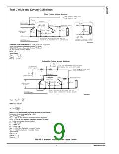
Test Circuit and Layout Guidelines
(Continued)
As in any switching regulator, layout is very important. Rap-
idly switching currents associated with wiring inductance can
generate voltage transients which can cause problems. For
minimal inductance and ground loops, the wires indicated by
heavy lines should be wide printed circuit traces and
should be kept as short as possible. For best results,
external components should be located as close to the
switcher lC as possible using ground plane construction or
single point grounding.
When using the adjustable version, special care must be
taken as to the location of the feedback resistors and the
associated wiring. Physically locate both resistors near the
IC, and route the wiring away from the inductor, especially an
open core type of inductor. (See application section for more
information.)
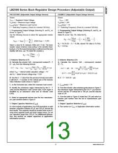
LM2598 Series Buck Regulator Design Procedure (Fixed Output)
PROCEDURE (Fixed Output Voltage Version)
Given:
EXAMPLE (Fixed Output Voltage Version)
Given:
VOUT = 5V
IN(max) = 12V
VOUT = Regulated Output Voltage (3.3V, 5V or 12V)
VIN(max) = Maximum DC Input Voltage
V
ILOAD(max) = Maximum Load Current
ILOAD(max) = 1A
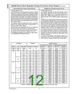
1. Inductor Selection (L1)
1. Inductor Selection (L1)
A. Select the correct inductor value selection guide from
Figures Figure 4, Figure 5, or Figure 6 (Output voltages of
3.3V, 5V, or 12V respectively.) For all other voltages, see the
design procedure for the adjustable version.
A. Use the inductor selection guide for the 5V version shown
in Figure 5.
B. From the inductor value selection guide, identify the in-
ductance region intersected by the Maximum Input Voltage
line and the Maximum Load Current line. Each region is
identified by an inductance value and an inductor code
(LXX).
B. From the inductor value selection guide shown in Figure 5,
the inductance region intersected by the 12V horizontal line
and the 1A vertical line is 68 µH, and the inductor code is
L30.
C. Select an appropriate inductor from the four manufactur-
er’s part numbers listed in Figure 8.
C. The inductance value required is 68 µH. From the table in
Figure 8, go to the L30 line and choose an inductor part
number from any of the four manufacturers shown. (In most
instance, both through hole and surface mount inductors are
available.)
2. Output Capacitor Selection (COUT
)
2. Output Capacitor Selection (COUT)
A. In the majority of applications, low ESR (Equivalent Series
Resistance) electrolytic capacitors between 47 µF and 330
µF and low ESR solid tantalum capacitors between 56 µF
and 270 µF provide the best results. This capacitor should be
located close to the IC using short capacitor leads and short
copper traces. Do not use capacitors larger than 330 µF.
A. See section on output capacitors in application infor-
mation section.
For additional information, see section on output capaci-
tors in application information section.
www.national.com
10

 NSC [ National Semiconductor ]