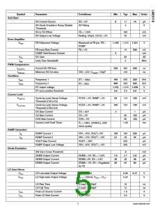
Symbol
Soft Start
Parameter
Conditions
Min
8
Typ
Max
14
Units
SS Current Source
SS = 0V
11
3
µA
V
SS Diode Emulation Ramp Disable
Threshold
SS Rising
SS to FB Offset
FB = 1.25V
160
45
mV
mV
SS Output Low Voltage
Sinking 100µA, UVLO = 0V
Error Amplifier
VREF
FB Reference Voltage
Measured at FB pin, FB =
COMP
1.195
3
1.215 1.231
V
FB Input Bias Current
COMP Sink/Source Current
DC Gain
FB = 2V
15
500
nA
mA
dB
AOL
fBW
80
3
Unity Gain Bandwidth
MHz
PWM Comparators
tHO(OFF)
Forced HO Off-time
320
450
100
580
ns
ns
tON(min)
Minimum HO On-time
VIN = 42V, CRAMP = 50pF
Oscillator
fSW1
Frequency 1
180
480
200
535
220
590
kHz
kHz
V
RT = 16kΩ
RT = 5kΩ
fSW2
Frequency 2
RT output voltage
RT sync positive threshold
1.191
3.0
1.215 1.239
3.5
4.0
V
Current Limit
VCS(TH)
Cycle-by-cycle Sense Voltage
Threshold (CSG-CS)
VCCX = 0V, RAMP = 0V
VCCX = 5V, RAMP = 0V
94
105
-1
110
122
126
139
mV
mV
VCS(THX)
Cycle-by-cycle Sense Voltage
Threshold (CSG-CS)
CS Bias Current
CS = 42V
CS = 0V
1
µA
µA
µA
ms
CS Bias Current
90
90
125
125
CSG Bias Current
Current Limit Fault Timer
CSG = 0V
1.28
RT = 16kΩ, (200kHz), (256
clock cycles)
RAMP Generator
IR1
IR2
RAMP Current 1
VIN = 40V, VOUT=10V
VIN = 10V, VOUT = 10V
VOUT = 36V
150
21
180
28
220
35
µA
µA
µA
mV
RAMP Current 2
VOUT Bias Current
RAMP Output Low Voltage
200
265
VIN = 40V, VOUT = 10V
Diode Emulation
SW Zero Cross Threshold
DEMB Output Current
DEMB Output Current
DEMB Output Current
-6
2.7
38
65
mV
µA
µA
µA
DEMB = 0V, SS = 1.25V
DEMB =0V, SS = 2.8V
1.6
28
45
3.8
48
85
DEMB = 0V, SS = Regulated
by FB
LO Gate Driver
VOLL
LO Low-state Output Voltage
LO High-state Output Voltage
ILO = 100mA
0.08
0.25
0.17
V
V
VOHL
ILO = -100mA, VOHL = VCC
VLO
-
LO Rise Time
C-load = 1000pF
C-load = 1000pF
VLO = 0V
18
12
ns
ns
A
LO Fall Time
IOHL
IOLL
Peak LO Source Current
Peak LO Sink Current
1.8
3.5
VLO = VCC
A
5
www.national.com

 NSC [ National Semiconductor ]