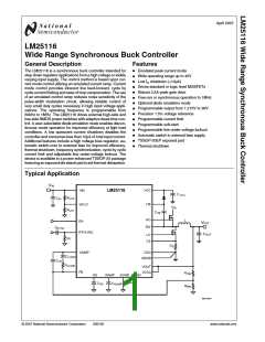
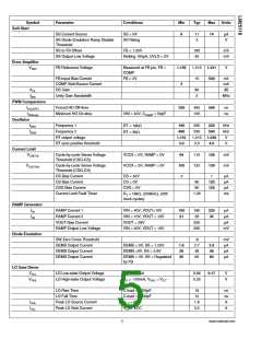
Connection Diagram
30015602
Top View
See NS Package Numbers MXA20A
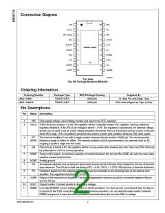
Ordering Information
Ordering Number
LM25116MH
Package Type
TSSOP-20EP
TSSOP-20EP
NSC Package Drawing
Supplied As
MXA20A
MXA20A
73 Units Per Anti-Static Tube
2500 units shipped as Tape & Reel
LM25116MHX
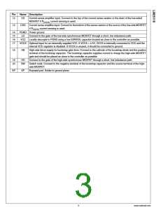
Pin Descriptions
Pin
Name Description
1
2
VIN Chip supply voltage, input voltage monitor and input to the VCC regulator.
UVLO If the UVLO pin is below 1.215V, the regulator will be in standby mode (VCC regulator running, switching
regulator disabled). If the UVLO pin voltage is above 1.215V, the regulator is operational. An external voltage
divider can be used to set an under-voltage shutdown threshold. There is a fixed 5µA pull up current on this pin
when EN is high. UVLO is pulled to ground in the event a current limit condition exists for 256 clock cycles.
3
RT/
The internal oscillator is set with a single resistor between this pin and the AGND pin. The recommended
SYNC frequency range is 50kHz to 1MHz. The internal oscillator can be synchronized to an external clock by AC
coupling a positive edge onto this node.
4
5
EN
If the EN pin is below 0.5V, the regulator will be in a low power state drawing less than 10µA from VIN. EN must
be pulled above 3.3V for normal operation.
RAMP Ramp control signal. An external capacitor connected between this pin and the AGND pin sets the ramp slope
used for current mode control.
6
7
AGND Analog ground.
SS
An external capacitor and an internal 10µA current source set the soft start time constant for the rise of the error
amp reference. The SS pin is held low during VCC < 4.5V, UVLO < 1.215V, EN input low or thermal shutdown.
8
9
FB
Feedback signal from the regulated output. This pin is connected to the inverting input of the internal error
amplifier. The regulation threshold is 1.215V.
COMP Output of the internal error amplifier. The loop compensation network should be connected between this pin
and the FB pin.
10
11
VOUT Output monitor. Connect directly to the output voltage.
DEMB Low-side MOSFET source voltage monitor for diode emulation. For start-up into a pre-biased load, tie this pin
to ground at the CSG connection. For fully synchronous operation, use an external series resistor between
DEMB and ground to raise the diode emulation threshold above the low-side SW on-voltage.
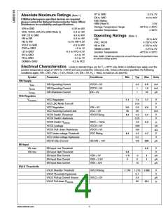
www.national.com
2

 NSC [ National Semiconductor ]